Cell, standard cell, standard cell library, a placement method using standard cell, and a semiconductor integrated circuit

a technology of cell and cell library, applied in the field of standard cell, a standard cell library and a placement method of standard cells, can solve the problems of deteriorating precision in the finished dimension of the gate electrode ultimately obtained, inability to apply the automatic placement in the foregoing manner, and reducing the cell area and chip area

Active Publication Date: 2006-06-22
SOCIONEXT INC
View PDF15 Cites 178 Cited by
  • Summary
  • Abstract
  • Description
  • Claims
  • Application Information

AI Technical Summary

Benefits of technology

[0018] Therefore, a main object of the present invention is to provide a semiconductor integrated circuit capable of reducing a cell area and a chip area.

Problems solved by technology

However, the regions R1, R2 and R3, which are only provided exclusively for the adjustment in the conventional technology, are normally unnecessary and do not include any device required for a circuit such as a transistor and wiring.
However, the automatic placement in the foregoing manner cannot be applied when a plurality of cells to be placed include non-identical cells and are designed so that their widths are arbitrary.
Further, as the miniaturization of the process, a precision in a finished dimension of the gate electrode ultimately obtained is deteriorated by an optical proximity effect when an interval between the gate electrodes and gate lengths of the gate electrodes are irregular in their patterns.
When the precision in the finished dimension of the gate electrode is deteriorated, performances of respective transistors of the semiconductor integrated circuit are increasingly inconstant, which leads to an increased variation in a performance of the semiconductor integrate circuit.
In order to solve aforementioned problems, The OPC (optical proximity effect correction) has been widely adopted in each transistor as a conventional technology, however, it takes a larger amount of time to process the OPC in each transistor.
However, as described, when the regions R1, R2 and R3 for adjusting the cell width to the integral multiple of the routing grid interval are provided, the gate electrode located on the cell boundary of the standard cell cannot be shared.
There is a possibility that the dummy electrodes DG are located with less than a minimum interval allowed in a design rule therebetween, which results in an error in the design rule.
Though the gate interval in each standard cell can be maintained at the constant level when such the gate length enlargement is executed, the gate length becomes irregular at the dummy gate electrodes DG2, which results in the imprecision of the finished dimension of the gate electrodes.
Further, the OPC cannot be processed in each standard cell due to the different gate lengths in the dummy gate electrodes DG in each standard cell and the dummy gate electrodes DG2 adjacent thereto.
As a result, the OPC cannot be processed in each standard cell.

Method used


Image

  • Cell, standard cell, standard cell library, a placement method using standard cell, and a semiconductor integrated circuit
  • Cell, standard cell, standard cell library, a placement method using standard cell, and a semiconductor integrated circuit
  • Cell, standard cell, standard cell library, a placement method using standard cell, and a semiconductor integrated circuit

Examples


embodiment 1

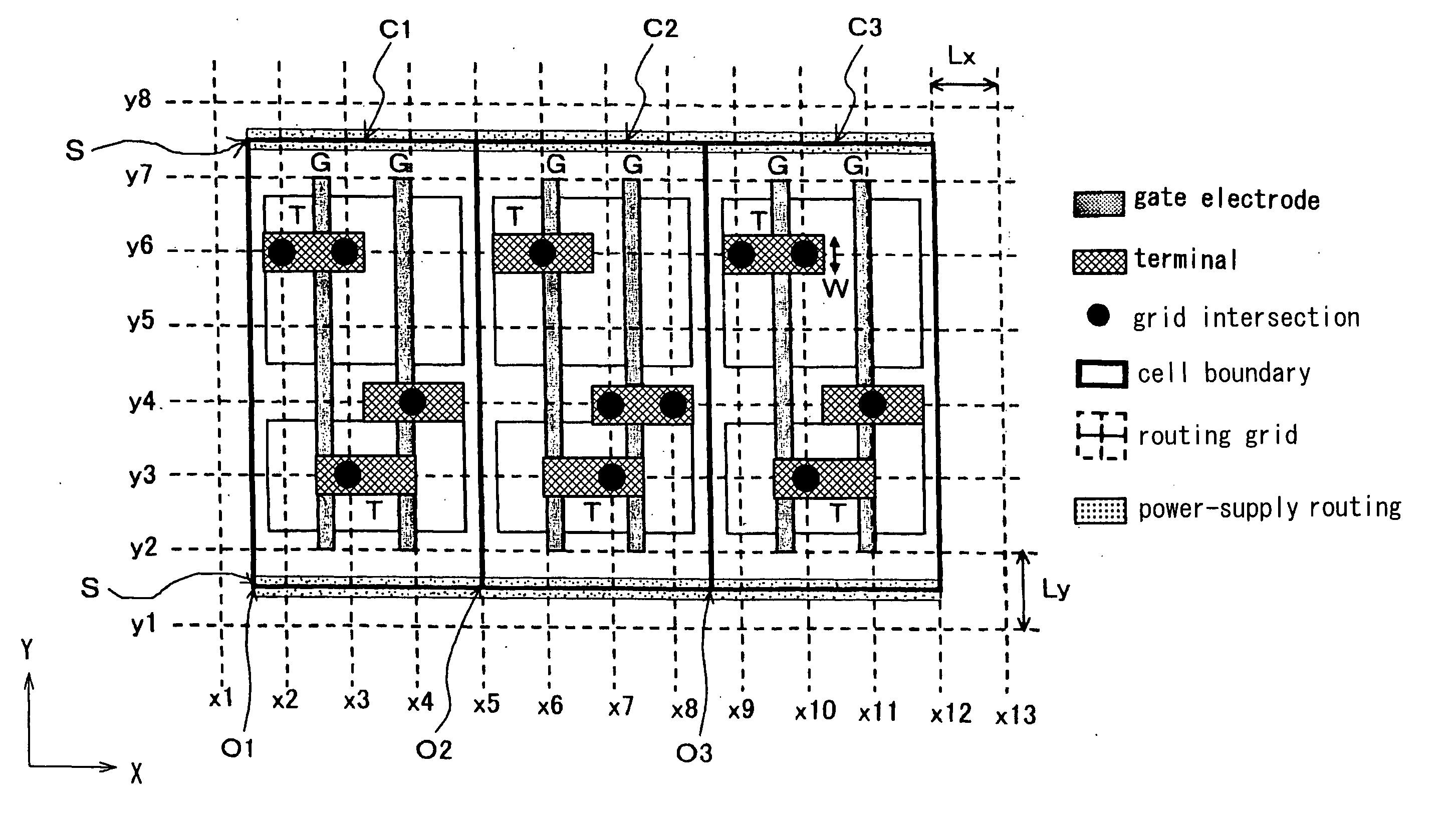
[0078]FIG. 1 is a layout of standard cells according to an embodiment 1 of the present invention. A direction along a power-supply wiring S of the standard cell is referred to as X direction, while a direction vertical to the power-supply wiring S is referred to as Y direction. The power-supply wiring S is merely an example, and is not necessarily allocated as shown.

[0079] Referring to reference symbols in FIG. 1, x1-x13 denote routing grids used in automatic placement & routing and provided in the X direction, y1-y8 denote routing grids provided in the Y direction, C1, C2 and C3 denote standard cells, O1, O2 and O3 are respectively origins of C1, C2 and C3, T denotes a terminal capable of transmitting an input signal or an output signal of a standard cell Ci (i=1, 2, . . . ), and G denotes a gate electrode.

[0080] An automatic placement & routing tool is an automatic design tool for determining the location of cells and blocks and routing path among their terminals. The automatic ...

embodiment 2

[0091]FIG. 5 is a design flow chart of an automatic placement & routing method using a standard cell according to an embodiment 2 of the present invention.

[0092] An automatic placement & routing apparatus for implementing the automatic placement& routing method comprises a connection information inputting device for acquiring a connection information of a logic circuit from outside, a design constraint inputting device for acquiring a design constraint of the logic circuit from outside, a layout information inputting device for acquiring a layout information of the standard cell from outside, a tentative placing device for tentatively placing respective cells based on the acquired connection information, and a relocating device for relocating the cells tentatively placed so as to reduce an area. The automatic placement & routing apparatus thus constituted places and routes the logic circuit including a plurality of standard cells.

[0093] First, the circuit connection information of...

embodiment 3

[0100]FIG. 7 is a design flow chart of an automatic placement & routing method using a standard cell according to an embodiment 3 of the present invention.

[0101] An automatic placement & routing apparatus for implementing the automatic placement & routing method comprises a connection information inputting device for acquiring a connection information of a logic circuit from outside, a design constraint inputting device for acquiring a design constraint of the logic circuit from outside, a layout information inputting device for acquiring a layout information of the standard cell from outside, a placing device for placing cells based on the acquired connection information, a tentative routing processing device for providing a tentative routing for connecting terminals of the respective cells, a terminal shape processing device. for shaping a terminal, and an actual routing processing device.

[0102] First, the circuit connection information of the logic circuit for connecting a plur...


PUM


Abstract

A cell according to the present invention comprises a plurality of terminals capable of transmitting an input signal or an output signal and serving as a minimum unit in designing a semiconductor integrated circuit, wherein the plurality of terminals is located on routing grids lined in a Y direction which is a direction vertical to a power-supply wiring of the cell used in automatic placement & routing and has a shape extended in an X direction which is a direction in parallel with the power-supply wiring, more specifically such a shape that, for example, a longer-side dimension of the terminal is equal to “a routing grid interval in the X direction+a wiring width. According to the constitution, a cell area is reduced, which advantageously leads to the reduction of a chip area.

Description

BACKGROUND OF THE INVENTION [0001] 1. Field of the Invention [0002] The present invention relates to a standard cell, a standard cell library and a placement method of standard cells for higher integration and area reduction. [0003] 2. Description of the Related Art [0004] In the layout design of LSI using an automatic placement & routing tool with on-grid design scheme, terminals of a cell for the communication of input / output signals must be located at the intersections of routing grids in the X and Y directions. In order to satisfy the demand, it is necessary to set a height of the cell to an integral multiple of an interval between the routing grids lined in the Y direction and to set a width of the cell an integral multiple of an interval between the routing grids lined in the X direction. Otherwise, the terminals may not locate at the grid intersection when the cells are placed adjacently with no spacing therebetween. The X direction denotes a direction along a power-supply ro...

Claims


Application Information

Patent Timeline
Patent Type & Authority Applications(United States)
IPC IPC(8): G06F17/50G06F9/45
CPCG06F17/5072H01L27/11807G06F30/392
Inventor ICHIRYU, MIWAMORIWAKI, TOSHIYUKITOUBOU, TETSUROU
Owner SOCIONEXT INC
Why Eureka
Try Eureka