

Photoanode using carbon nanotubes, method of manufacturing the photoanode, and photovoltaic solar cell including the photoanode
a carbon nanotube and photoanode technology, applied in the field of solar cells including carbon nanotubes, can solve the problems of increasing resistance, reducing the commercial application of silicon solar cells, and requiring high-purity silicon
- Summary
- Abstract
- Description
- Claims
- Application Information
AI Technical Summary
Problems solved by technology
Method used
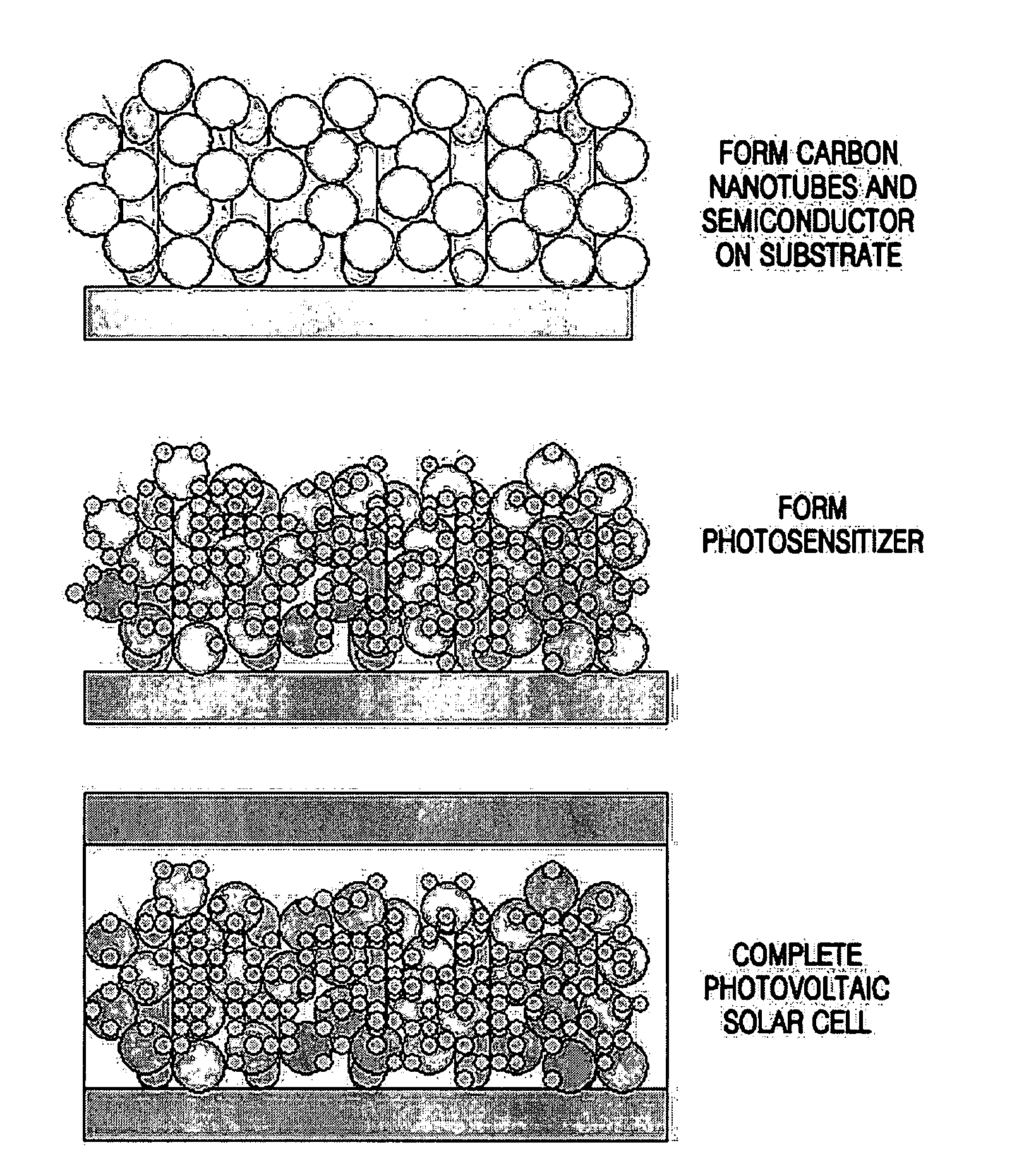
Image

Examples
example 1
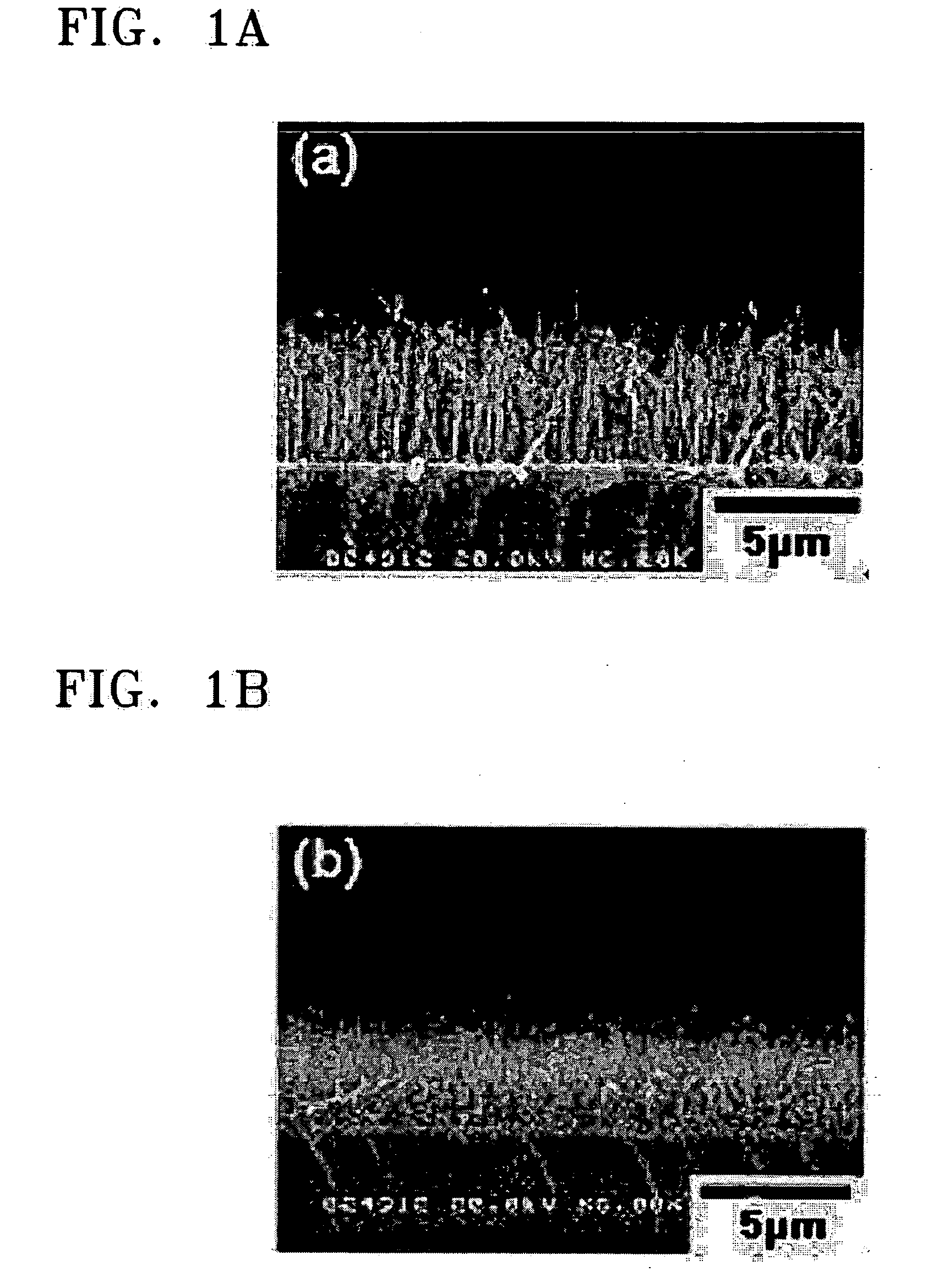
[0055] First, an Invar layer, which was a metal catalyst layer, was formed to a thickness of 1 to 10 nm using sputtering on a transparent and conductive glass substrate coated with ITO and having a transmittance of 80%.
[0056] Next, carbon nanotubes were grown vertically on the conductive substrate using plasma CVD in a hot filament plasma-enhanced CVD (HFPECVD) system (Mat Sci Tech model CNT-2000). Ammonia and acetylene were used as carbon source gases. During the growth of the carbon nanotubes, a substrate temperature was maintained at 5000, and a chamber pressure was maintained at 3.2 Torr. The gas flow rates of ammonia and acetylene were kept 120 sccm (standard cubic centimeter per minute) and 30 sccm, respectively, and a total growth time was 20 minutes at a bias voltage of 580V and a filament current of 11.1 A.
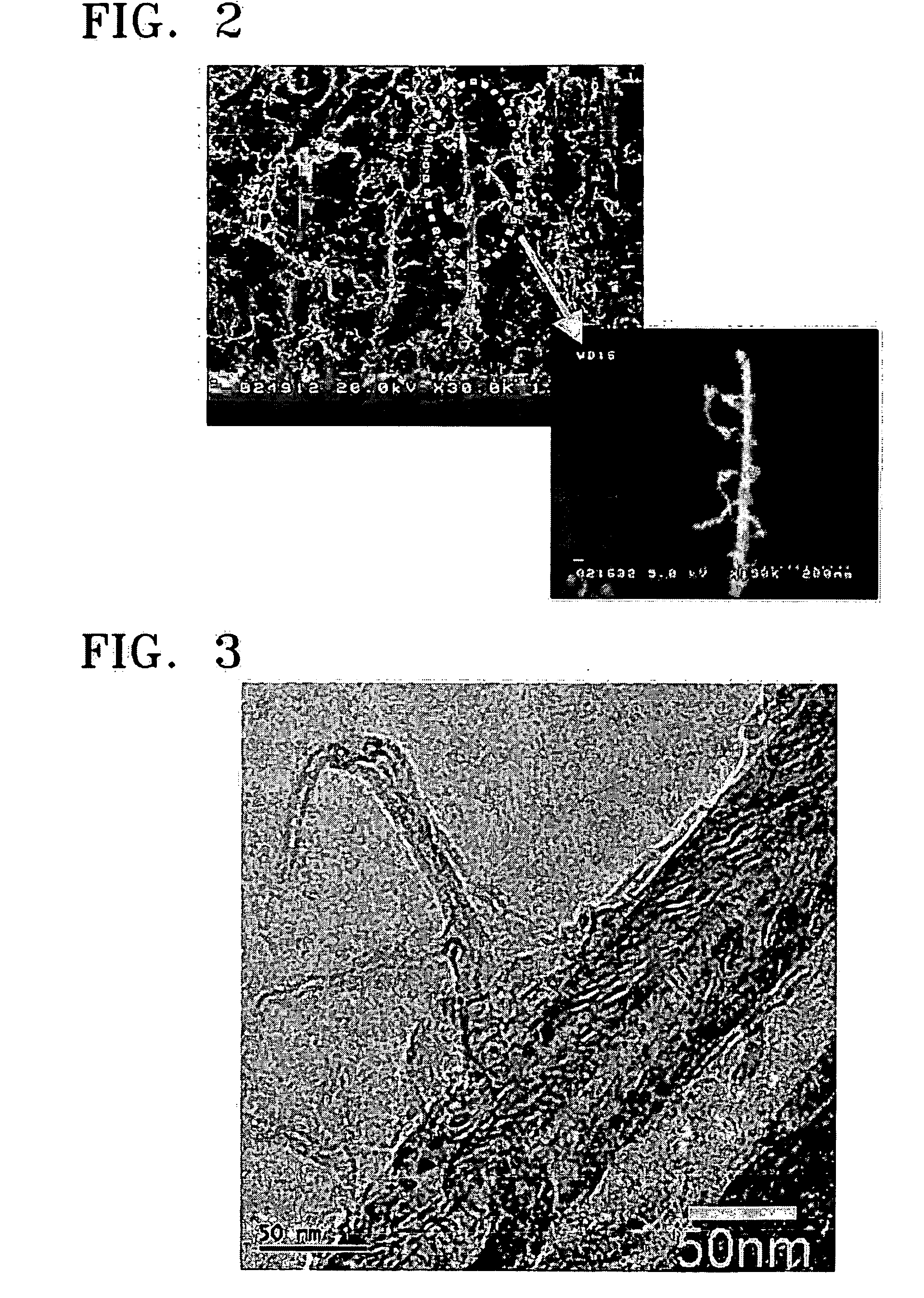
[0057] Next, carbon nanotubes were grown using thermal CVD to obtain branched carbon nanotubes. GNCVD300 was used as a thermal CVD system, and hydrogen and carbon monox...
example 2
[0061] A photoanode was manufactured in the same manner as in Example 1 except that the forming of carbon nanotubes using thermal CVD was omitted.
PUM
| Property | Measurement | Unit |
|---|---|---|
| transmittance | aaaaa | aaaaa |
| thickness | aaaaa | aaaaa |
| conductive | aaaaa | aaaaa |
Abstract
Description
Claims
Application Information