Method for manufacturing a semiconductor device

a manufacturing method and semiconductor technology, applied in the direction of solid-state devices, transistors, electric devices, etc., can solve the problem that the thermal budget of high-voltage operation devices cannot be applied to the process, and achieve the effect of reducing the number of masks and relevant processing steps, enhancing the productivity of the total process of the device, and reducing the total time of manufacturing

Inactive Publication Date: 2006-06-29
COLUMBA TECH INC
View PDF14 Cites 22 Cited by
  • Summary
  • Abstract
  • Description
  • Claims
  • Application Information

AI Technical Summary

Benefits of technology

[0021] According to the present invention, an additional mask that was conventionally employed for forming the extended drain region of the HV DECMOS device is replaced with a mask for forming a logic well. Therefore, the extended drain region and the logic well may be simultaneously formed in a single process with the use of the same mask, and the number of masks and relevant processing steps may be reduced. Consequently, productivity of the total process of the device can be enhanced and / or the total time of manufacturing can be reduced. In addition, in an LCD Driver IC (LDI) process wherein devices for HV / MV / LV operation are merged or combined, a one-chip solution can replace a two-chip or three-chip solution, so the process can be simplified. Therefore, the cost of the semiconductor device can be reduced.

Problems solved by technology

This is because the thermal budget for the high voltage operation device cannot be applied to the process for making a low voltage or a medium voltage operation device.

Method used


Image

  • Method for manufacturing a semiconductor device
  • Method for manufacturing a semiconductor device
  • Method for manufacturing a semiconductor device

Examples


Embodiment Construction

[0025] An exemplary embodiment of the present invention will hereinafter be described in detail with reference to the accompanying drawings.

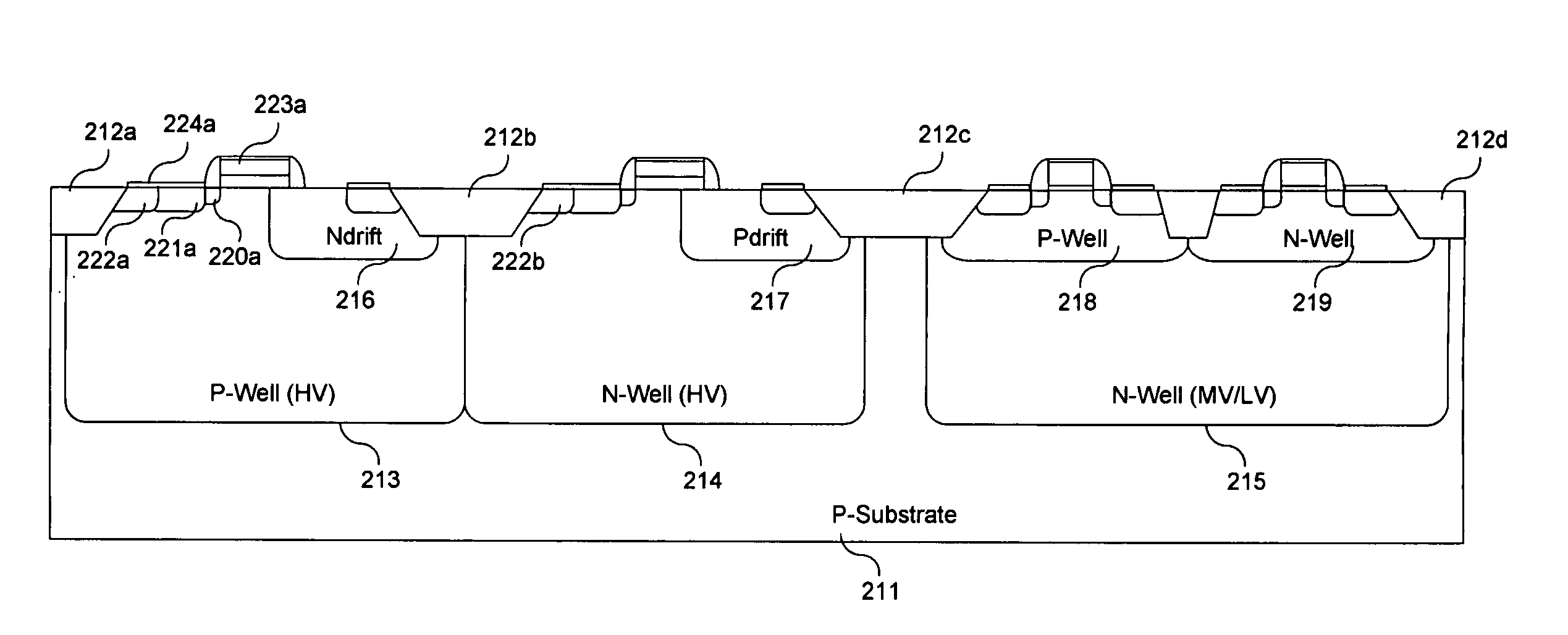
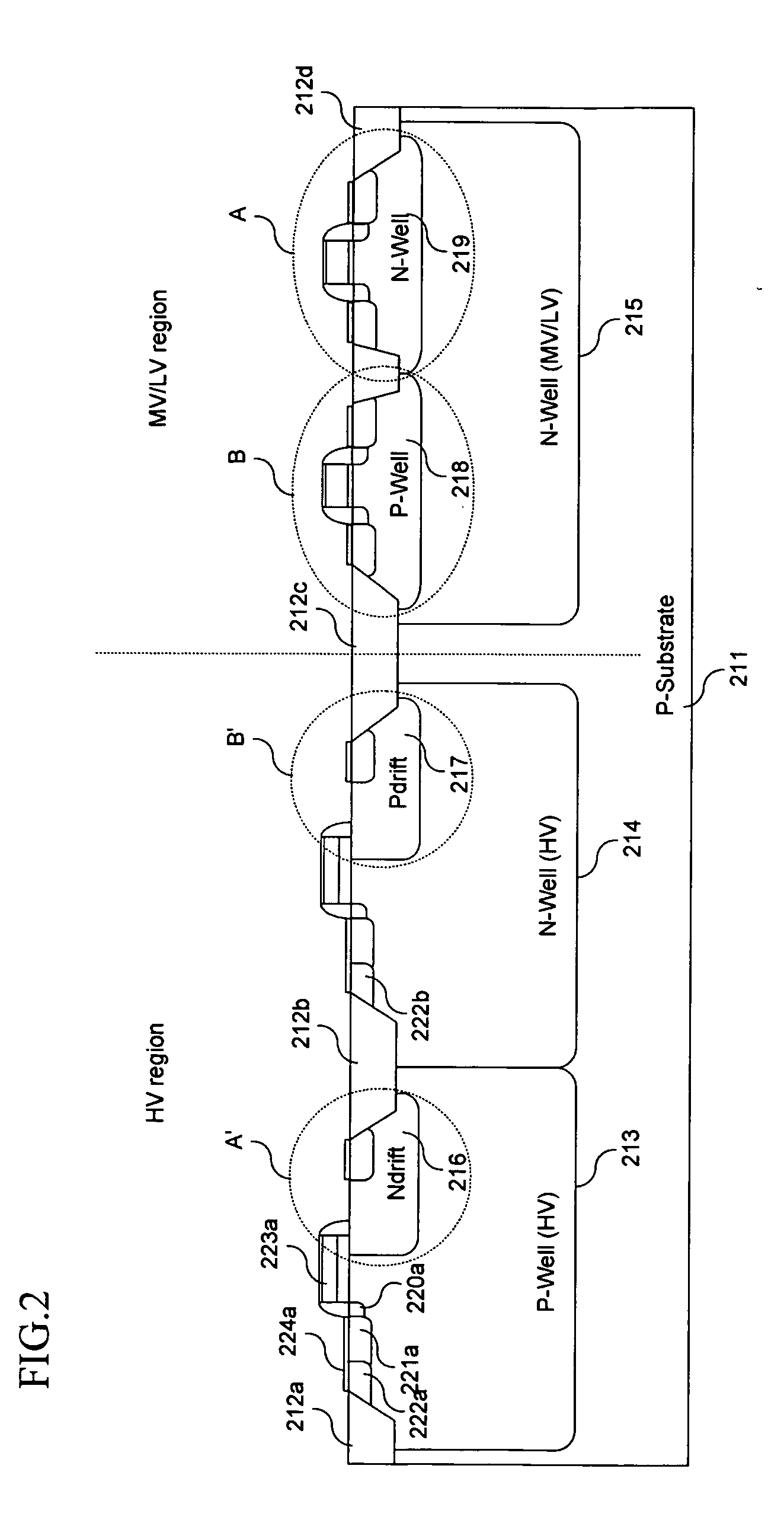
[0026] Recently, a conventional process for forming a high voltage (HV) semiconductor device (and / or one or more junctions thereof has been replaced with a simultaneous process for forming a retrograde well by high energy ion implantation.

[0027] In a semiconductor device for a one-chip solution IC used for driving a display panel (e.g., a thin film transistor (TFT) LCD, an organic light emitting diode (OLED), etc.), a device configured to operate at low voltage (a so-called LV device), a device configured to operate at medium voltage (a so-called MV device), and a device configured to operate at high voltage (a so-called HV device) are desired for a panel driver or for constituent elements in such a one-chip solution IC. Although not limited to any particular operational voltages, the LV device may operate in a range of from 0 to 5 V (i.e., us...


PUM


Abstract

An exemplary method of manufacturing a semiconductor device according to an embodiment of the present invention includes forming a P-well and an N-well for high voltage (HV) devices and a first well in a low voltage/medium voltage (LV/MV) region for a logic device, in a semiconductor substrate; simultaneously forming a second well in the LV/MV region for a logic device and a drift region for one of the HV devices using the same mask; and respectively forming gate oxide layers on the semiconductor substrate in the HV/MV/LV regions. According to the present invention, the number of photolithography processes can be reduced by replacing or combining an additional mask for forming an extended drain region of a high voltage depletion-enhancement CMOS (DECMOS) with a mask for forming a typical well of a logic device, so productivity of the total process of the device can be enhanced.

Description

CROSS-REFERENCE TO RELATED APPLICATION [0001] This application claims priority to and the benefit of Korean Patent Application No. 10-2004-0115641, filed in the Korean Intellectual Property Office on Dec. 29, 2004, the entire contents of which are incorporated herein by reference. BACKGROUND OF THE INVENTION [0002] (a) Field of the Invention [0003] The present invention relates to a method of manufacturing a semiconductor device. In more detail, the present invention relates to a method of manufacturing a semiconductor device (including a combination of high voltage (HV) depletion-enhancement CMOS (DECMOS) devices and logic devices) that is capable of simultaneously forming medium voltage (MV) and high voltage devices. [0004] (b) Description of the Related Art [0005] In a process for manufacturing a liquid crystal display driver integrated circuit (LCD Driver IC, or LDI) according to a conventional art, a controller IC, a source driver IC, and a gate driver IC are usually formed as ...

Claims


Application Information

Patent Timeline
Patent Type & Authority Applications(United States)
IPC IPC(8): H01L21/8234
CPCH01L21/823814H01L21/823857H01L21/823892H01L21/18
Inventor LEE, KYUNG-HO
Owner COLUMBA TECH INC
Why Eureka
Try Eureka