Gas manifold valve cluster

a gas manifold valve and cluster technology, applied in the direction of vacuum evaporation coating, chemical vapor deposition coating, coating, etc., can solve the problems of large reaction volume, large reaction volume, and complex calculation of coo, so as to reduce the length and volume of gas lines, minimize the time required, and increase the productivity of the process chamber

Inactive Publication Date: 2007-02-08
AVIZA TECHNOLOGY INC
View PDF44 Cites 8 Cited by
  • Summary
  • Abstract
  • Description
  • Claims
  • Application Information

AI Technical Summary

Benefits of technology

[0012] The present invention relates generally to a deposition apparatus for semiconductor processing. More specifically, embodiments of the present invention relate to a gas manifold valve cluster and deposition apparatus. In some embodiments of the present invention a gas manifold valve cluster and system are provided that promotes reduced length and volumes of gas lines that will be exposed to atmosphere during cleaning which minimizes the time required to perform process chamber maintenance and therefore increase the productivity of the process chamber. In other embodiments a gas manifold valve cluster and system are provided that promote fast actuation of gases during semiconductor processing, particularly during atomic layer deposition (ALD). In some embodiments of the present invention, chemical precursor pulse times in an ALD cycle have been reduced by up to 50% as compared to prior art pulse times.
[0013] Embodiments of the present invention may be used to practice process methods on a semiconductor substrate, such as but not limited to: thin film deposition techniques such as CVD, PVD, and ALD, etching, ashing, cleaning, and the like. In some embodiments the gas manifold valve cluster and system promote one or more of: more efficient use of the gas, reduction in the sources of contamination, facilitating uniform gas flow pattern, facilitating fast gas exchange, and easier chamber cleaning.

Problems solved by technology

The calculation of COO is very complex.
In such prior art systems this reaction volume is relatively large.
One major drawback of this configuration is that the slot valve and wafer transfer region through which the wafers are transported are also exposed to the reaction zone.
This results in the deposition of materials, particles, and contaminants in the slot valve region.
This also results in plasma field asymmetries for process methods that use a plasma energy source.
Further, this wafer transfer region causes temperature non-uniformities during processing.
The region tends to have a black body cavity effect and the area of the heater that is adjacent this region develops cold regions, thus causing uneven heating and processing of the wafer.
Thus, known process chamber designs suffer from a number of shortcomings.
Reaction volumes tend to be excessively large relative to the volume of the cylinder defined by the diameter of substrate support.
The walls of such process chambers are often not symmetrical due to the requirement for additional ports, substrate transfer openings and the like.
This leads to undesirable effects including one or more of: long evacuation times, excessive chemical usage, long purge times, long cycle times for ALD process methods, asymmetric gas flow, particle generation, asymmetric plasma densities for plasma process methods, material deposits on the walls of the process chamber, shorter times between cleaning the process chamber, and the like.
This time is costly in that the process chamber is not productive during the maintenance period.
These designs suffer from several drawbacks.

Method used


Image

  • Gas manifold valve cluster
  • Gas manifold valve cluster
  • Gas manifold valve cluster

Examples


Embodiment Construction

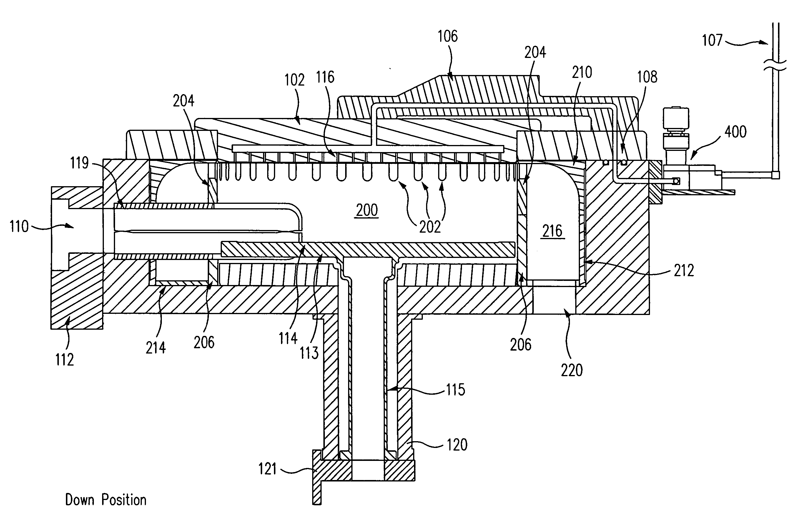
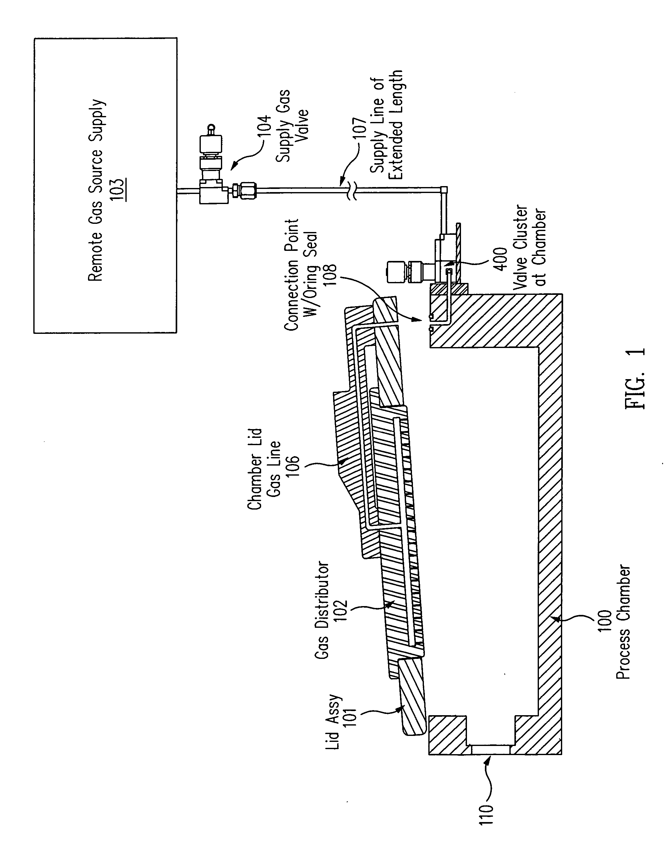
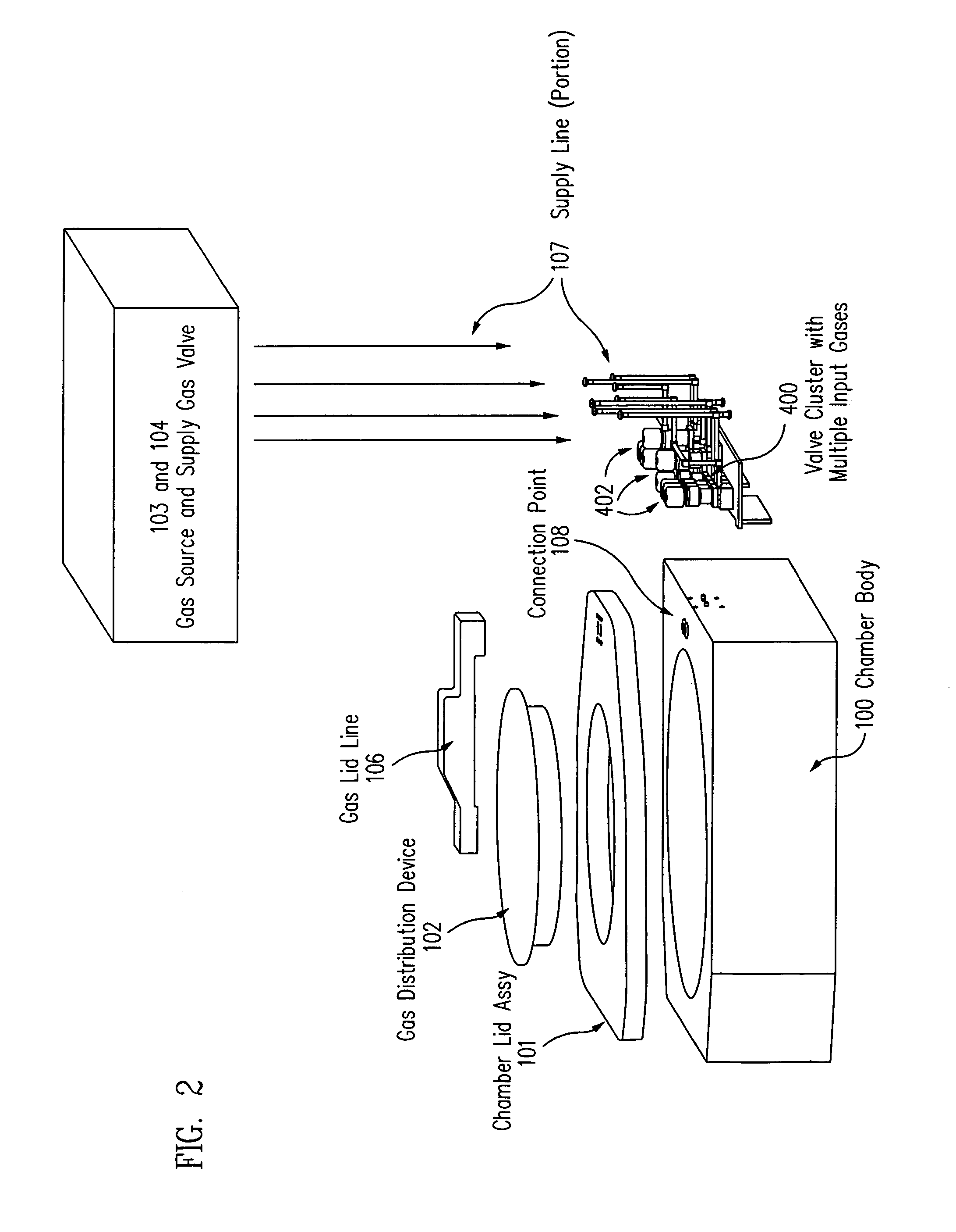
[0024] The present invention relates generally to a deposition apparatus for semiconductor processing. More specifically, embodiments of the present invention relate to a gas manifold valve cluster and deposition apparatus.

[0025]FIG. 1 illustrates a cross sectional simplified view of one embodiment of the gas manifold valve cluster and deposition apparatus of the present invention. FIG. 2 depicts a three-dimensional exploded view of embodiments of the gas manifold valve cluster and deposition apparatus of the present invention. FIG. 6 shows a top plan view of embodiments of the gas manifold valve cluster and deposition apparatus It will be appreciated by those skilled in the art that embodiments of the present invention are applicable to a wide variety of process methods such as chemical vapor deposition (CVD), atomic layer deposition (ALD), physical vapor deposition (PVD), Epi, etching, ashing, rapid thermal processing (RTP), short thermal processes such as spike anneal, and the l...


PUM

PropertyMeasurementUnit
temperatureaaaaaaaaaa
lengthaaaaaaaaaa
volumeaaaaaaaaaa

Abstract

The present invention relates generally to a deposition apparatus for semiconductor processing. More specifically, embodiments of the present invention relate to a gas manifold valve cluster and deposition apparatus. In some embodiments of the present invention a gas manifold valve cluster and system are provided that promotes reduced length and volumes of gas lines that will be exposed to atmosphere during cleaning which minimizes the time required to perform process chamber maintenance and therefore increase the productivity of the process chamber. In other embodiments a gas manifold valve cluster and ALD deposition apparatus are provided.

Description

CROSS REFERENCE TO RELATED APPLICATIONS [0001] This application claims the benefit of, and priority to, U.S. Provisional Patent Application Ser. No. 60 / 703,711 filed on Jul. 29, 2005, 60 / 703,717 filed on Jul. 29, 2005 and 60 / 703,723 filed on Jul. 29, 2005, the entire disclosures of all of which are hereby incorporated by reference. This application is related to co-pending United States Utility Patent Application corresponding to Attorney Docket no. 186440 / US / 2 / MSS, filed concurrently herewith, the entire disclosure of which is hereby incorporated by reference.FIELD OF THE INVENTION [0002] The invention relates generally to a deposition apparatus for semiconductor processing. More specifically, the invention relates to a gas manifold valve cluster and deposition apparatus useful to perform various process methods to form thin films on a semiconductor substrate. BACKGROUND OF THE INVENTION [0003] The manufacture of semiconductor devices requires many steps to transform a semiconducto...

Claims


Application Information

Patent Timeline
Patent Type & Authority Applications(United States)
IPC IPC(8): C23C16/00C23C14/00
CPCC23C16/4401C23C16/4409C23C16/4412C23C16/455H01L21/67751C23C16/45536C23C16/45544C23C16/45561H01L21/6719C23C16/45525H01L21/205
Inventor BERCAW, CRAIGCOSSENTINE, DANYAO, JACKLO, TOMMYDEDONTNEY, JAYBARTHOLOMEW, LAWRENCECHATHAM, ROBERT
Owner AVIZA TECHNOLOGY INC
Why Eureka
Try Eureka