Light-emitting device, method of manufacturing the same, and display unit
- Summary
- Abstract
- Description
- Claims
- Application Information
AI Technical Summary
Benefits of technology
Problems solved by technology
Method used
Image

Examples
example 1
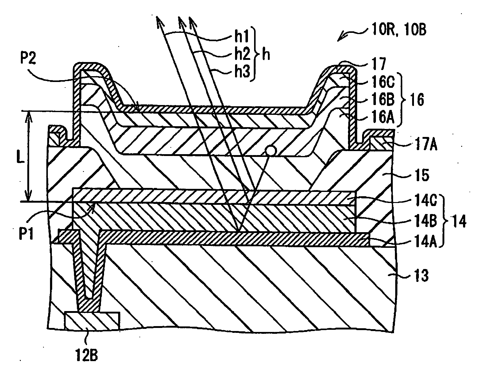
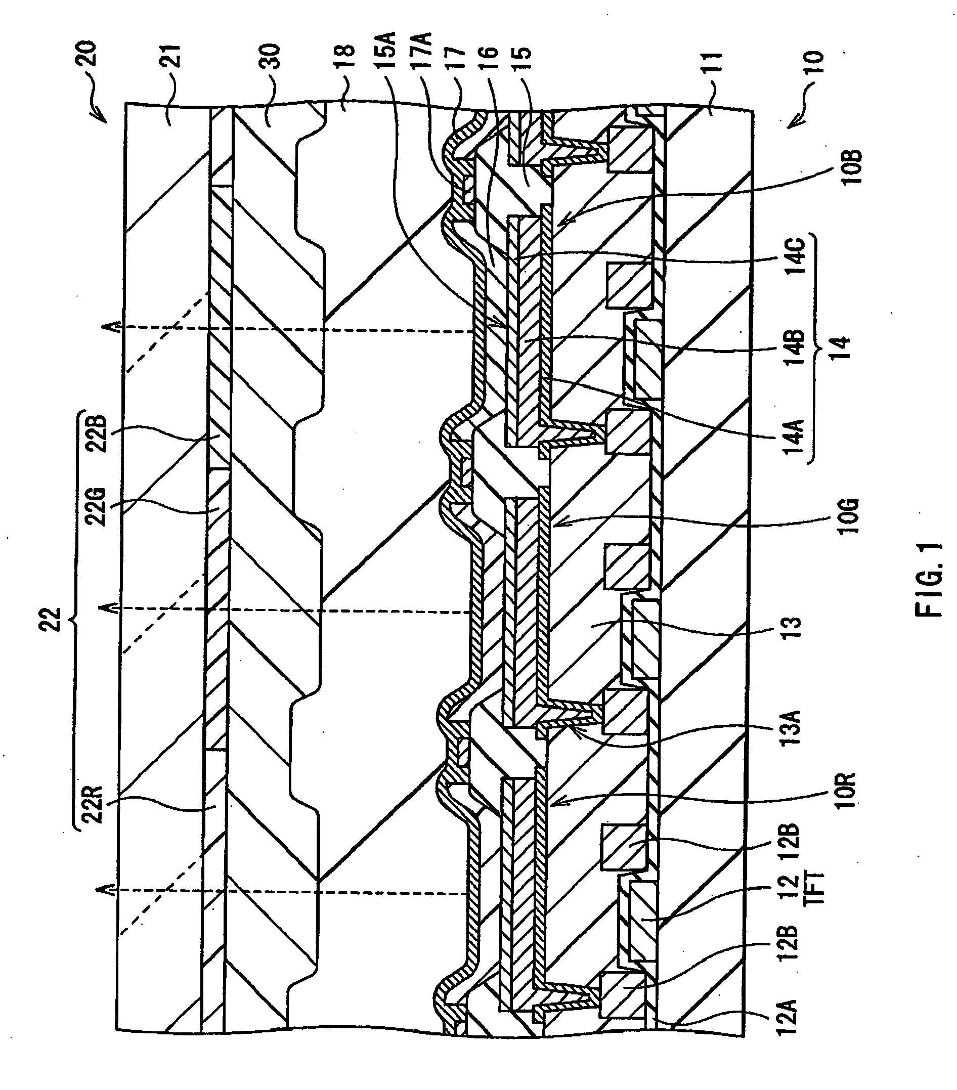
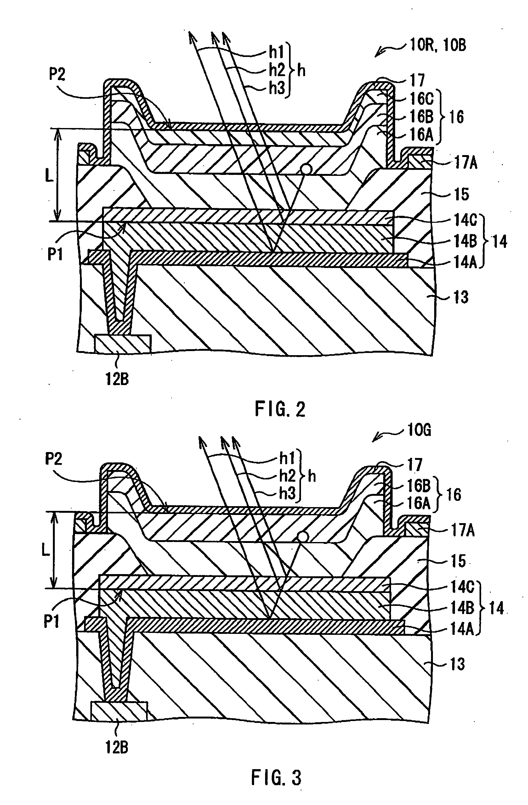
[0099] As in the case of the second embodiment, the organic light-emitting device was formed. At that time, the first electrode 14 had a structure in which the adhesive layer-cum-auxiliary reflective film 14D made of chromium with a thickness of about 40 nm, the reflective layer 14B made of an alloy including silver with a thickness of about 36 nm, and the barrier layer 14C made of ITO with a thickness of 7.5 nm were laminated. Moreover, the resonant wavelength of the above-described resonator (peak wavelength of the spectrum of light extracted from the second electrode 17) was set to about 400 nm and about 800 nm. In the obtained organic light-emitting device, the reflectance of the first electrode 14 in both cases was determined. The obtained results are shown in FIG. 17.
[0100] As Reference Examples 1 through 5 relative to the example, as shown in FIG. 18, a first electrode 114 which was equivalent to the example except that the first electrode 114 included only a reflective laye...
example 2
[0102] The first electrode 14 was formed as in the case of Example 1, except that the thickness of the adhesive layer 14A was about 150 nm. The reflectance thereof was determined, and the same results as those in Example 1 were obtained. The obtained results are shown in FIG. 17.
[0103] Although the present invention is described referring to the embodiments and the examples, the invention is not limited to the embodiments and the examples, and is variously modified. For example, the materials and the thicknesses of the layers, film forming methods, film forming conditions and so on are not limited to those described in the embodiments and the examples, and any other materials, any other thicknesses, any other film forming methods and any other film forming conditions may be applicable. For example, the adhesive layer 14A or the adhesive layer-cum-auxiliary reflective film 14D can be formed by not only sputtering, but also vapor deposition, CVD, MOCVD (metal organic chemical vapor d...
PUM
 Abstract
Description
Claims
Application Information
 - Generate Ideas
- Intellectual Property
- Life Sciences
- Materials
- Tech Scout
- Unparalleled Data Quality
- Higher Quality Content
- 60% Fewer Hallucinations
Browse by: Latest US Patents, China's latest patents, Technical Efficacy Thesaurus, Application Domain, Technology Topic, Popular Technical Reports.
© 2025 PatSnap. All rights reserved.Legal|Privacy policy|Modern Slavery Act Transparency Statement|Sitemap|About US| Contact US: help@patsnap.com