

Gallium nitride semiconductor device
a technology of gallium nitride and semiconductor devices, which is applied in the direction of semiconductor devices, electrical apparatus, transistors, etc., can solve the problems of excessive power loss in diodes, and achieve the effect of improving reliability and low manufacturing cos
- Summary
- Abstract
- Description
- Claims
- Application Information
AI Technical Summary
Benefits of technology
Problems solved by technology
Method used
Image

Examples
first embodiment
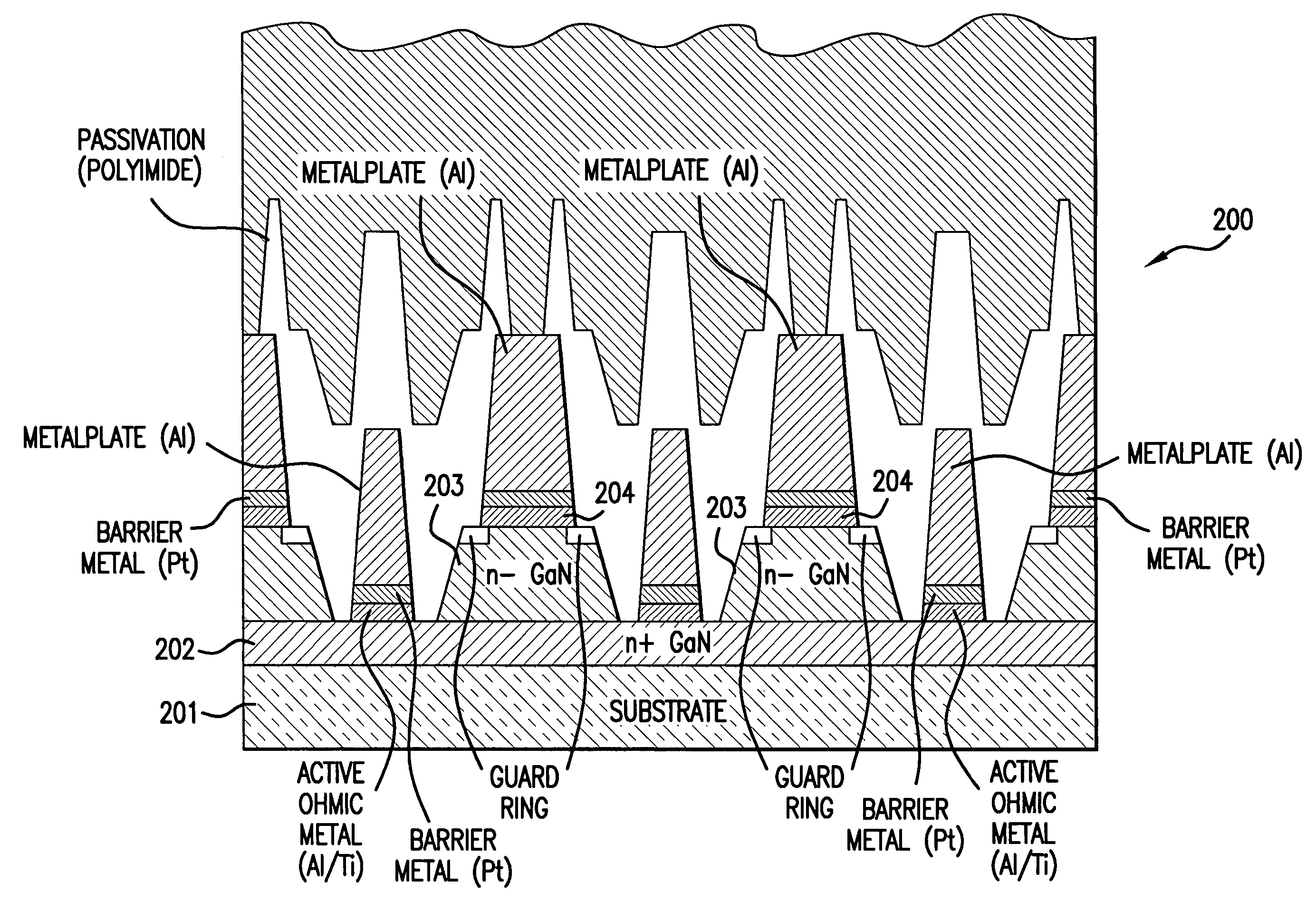
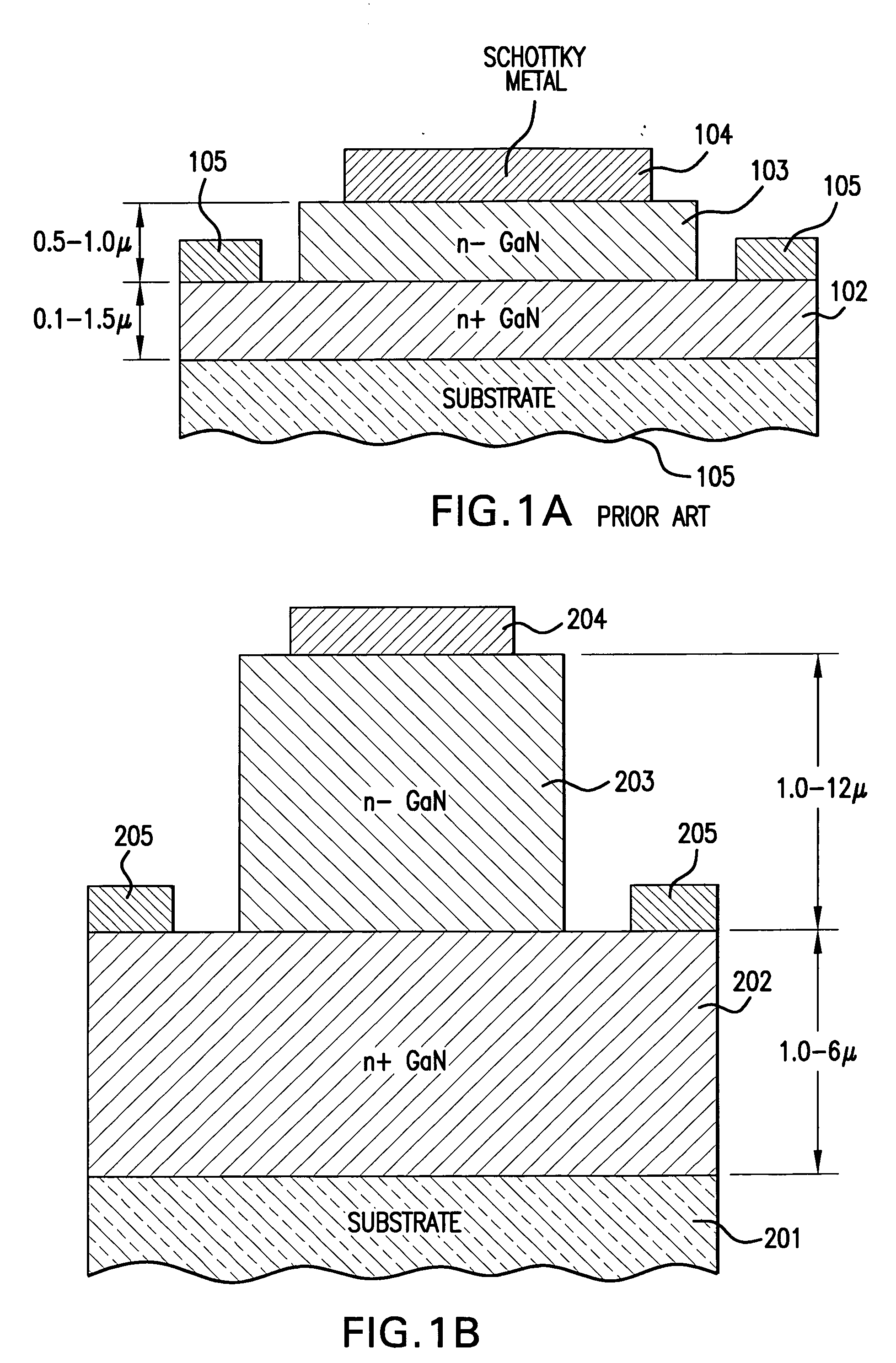
[0049]FIG. 1B shows a highly enlarged view of a Schottky diode 200 constructed in accordance with the present invention formed of the Group III nitride based material system. Group III nitrides refer to those semiconductor compounds formed between nitrogen and the elements in group III of the periodic table, usually aluminum (Al), gallium (Ga), and indium (In). The term also refers to ternary and tertiary compounds such as AlGaN and AlInGaN. The preferred materials for the new diode are GaN and AlGaN.
[0050] Unlike the prior art device shown in FIG. 1A, the diode 200 according to the present invention utilizes a substrate 201 that is preferably sapphire (Al2O3) due to its reduced cost and wide availability in many different diameters. Alternatively, a silicon substrate may be used.
[0051] The use of an insulating or sapphire substrate for semiconductor devices has generally relied on relatively thick sapphire substrates, such as 15 to 25 mils depending on diameter, which are commerci...
third embodiment
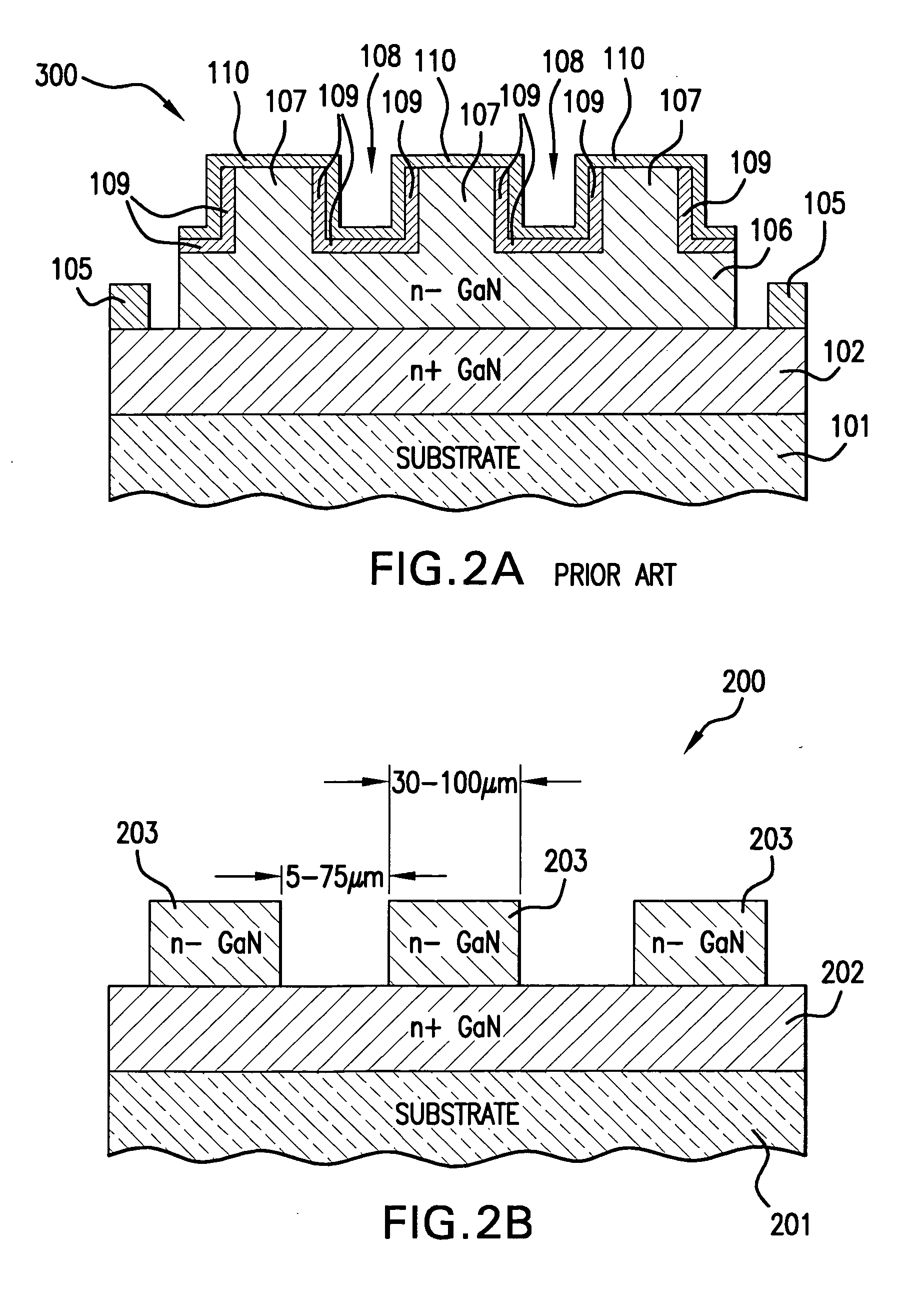
[0058]FIG. 3 is a highly simplified cross-sectional view of another GaN diode as known in the prior art in a third embodiment as depicted in US 2003 / 0062525; a trench structure to reduce reverse current. Like the Schottky diode depicted in FIG. 2A above, the trench structure separates a plurality of parallel, equally spaced trenches, but in this embodiment, the top layers are etched through the AlGaN barrier layer 111 and completely through the n− GaN layer 106, to the n+ GaN layer 102. Similar mesa regions are formed between adjacent trenches. The trench sidewalls and bottom surface have an insulation layer 109 with the top Schottky metal layer 110 covering the entire trench structure. The trench structure functions in the same way as the embodiment of FIG. 2A above, reducing the reverse current.
[0059]FIGS. 4A and 4B are a top plan views of the GaN diode according to the present invention in respective first and second embodiments of the upper layers of the device which provide alt...
second embodiment
[0062]FIG. 4B is an enlarged top plan view of the entire gallium nitride semiconductor device according to the present invention as implemented on a single die showing the ohmic 408, 409 wire-bonding contact regions on the die but utilizing a different approach to making the Schottky contacts that the approach used in FIG. 4A.
[0063] In particular, in the second embodiment a metal pad 410 extends over all of the mesa fingers and makes electrical contact with the Schottky metal. The metal pad 410 improves ability to wirebond larger diameter wires to the Schottky contact area when using relatively narrow and short device fingers. Additionally, the Schottky wirebond mesa pad areas shown in FIG. 4A can be completely removed from the center of the device as shown in FIG. 4B.
[0064]FIG. 5A is a detailed cross-sectional view of the GaN diode according to the present invention through the A-A plane of FIG. 4A showing depicting the mesa structure in greater detail.
[0065] In particular, there...
PUM
 Abstract
Description
Claims
Application Information