Semiconductor device and method for fabricating the same

Inactive Publication Date: 2006-07-06
PANASONIC CORP
View PDF10 Cites 76 Cited by
  • Summary
  • Abstract
  • Description
  • Claims
  • Application Information

AI Technical Summary

Benefits of technology

[0030] In the semiconductor device of the present invention, it is preferable that the interlevel insulation film is formed of silicon oxide containing carbon, fluorine or nitride. Thus, the interlevel insulation film contains silicon oxide as a main component, so that a semiconductor process using silicon can be easily adopted.
[0031]

Problems solved by technology

However, it is a problem of a low dielectric constant insulation film such as silicon oxide (SiOC) containing carbon that chemical, mechanical and thermal stability is lower than that of a known silicon dioxide (SiO2) film.
However, it

Method used


Image

  • Semiconductor device and method for fabricating the same
  • Semiconductor device and method for fabricating the same
  • Semiconductor device and method for fabricating the same

Examples


first embodiment

[0052] A first embodiment of the present invention will be described with reference to the accompanying drawings.

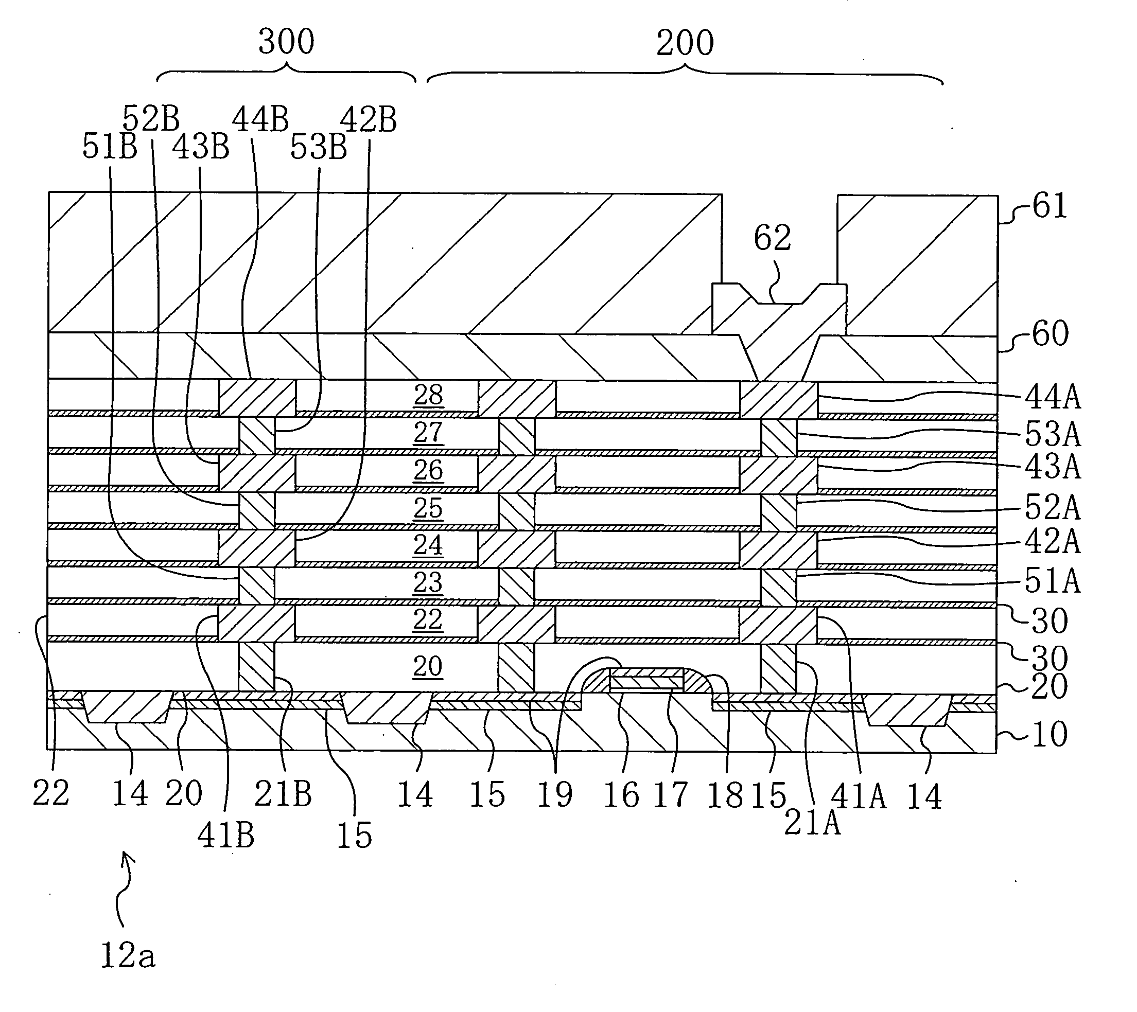
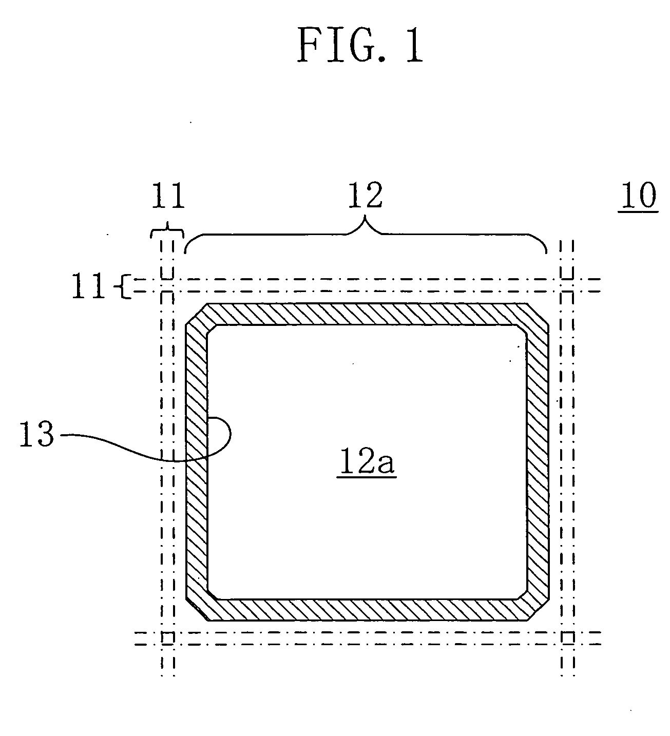
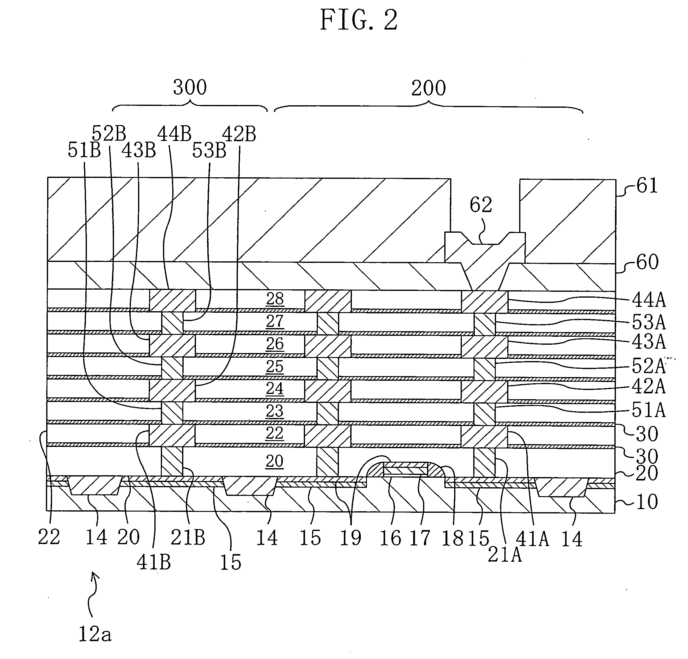
[0053]FIG. 1 is a view illustrating a planar structure of a chip formation region in a semiconductor wafer forming a semiconductor device according to the first embodiment of the present invention. As shown in FIG. 1, a chip region 12 is formed on a principal plane of a semiconductor substrate (semiconductor wafer) 10 so as to be surrounded by scribe regions 11 intersecting with one another. In an inner peripheral portion of the chip region 12, a seal ring 13 having a known structure is formed.

[0054] A semiconductor device according to the present invention is characterized in that a semiconductor element is provided in an element formation region 12a in part of the chip region 12 located inside of the seal ring 13.

[0055]FIG. 2 is a view partially illustrating a cross-sectional structure of the semiconductor device of the first embodiment of the present invention. As s...

second embodiment

[0077] Hereinafter, a second embodiment of the present invention will be described with reference to the accompanying drawings.

[0078]FIG. 5 is a view partially illustrating a cross-sectional structure of a semiconductor device according to a second embodiment of the present invention. In FIG. 5, each member also shown in FIG. 2 is identified by the same reference numeral and therefore the description thereof will be omitted.

[0079] The multilayer interconnect of the first embodiment as well as the dummy interconnect section 300 is formed by so-called single damascene in which an interconnect layer and a connection section (via) are separately formed. In the second embodiment, in contrast, dual damascene in which an interconnect layer and a connection section are formed as a unit is used to form the multilayer interconnect.

[0080] A mechanical stress generated in polishing the second interlevel insulation film 22 of a low dielectric constant material and the like by CMP is different...

first modified example of second embodiment

[0091] Hereinafter, a first modified example of the second embodiment of the present invention will be described with reference to the accompanying drawings.

[0092]FIG. 7 is a view partially illustrating a cross section of a semiconductor device according to the first modified example of the second embodiment of the present invention. In FIG. 7, each member also shown in FIG. 5 is identified by the same reference numeral and therefore the description thereof will be omitted.

[0093] As shown in FIG. 7, in the first modified example, a dummy contact is not formed between a first dummy interconnect 41B and a semiconductor substrate 10. That is, the first through fourth interconnects 41B through 44B are electrically floating.

[0094] Thus, with a dummy contact not provided in a dummy interconnection section 300, the degree of freedom of circuit design is improved and increase in a chip area can be suppressed.


PUM


Abstract

A semiconductor device includes a semiconductor element formed on a semiconductor substrate, a first interconnect formed over the semiconductor substrate so as to be electrically connected with the semiconductor element, and a second interconnect formed over the first interconnect with an interlevel insulation film made of an insulator having a lower dielectric constant than a dielectric constant of silicon oxide interposed between the first interconnect and the second interconnect. Furthermore, the semiconductor device includes a first dummy interconnect formed in part of the semiconductor substrate located in the vicinity of the first interconnect or the second interconnect.

Description

CROSS-REFERENCE TO RELATED APPLICATION [0001] The disclosure of Japanese Patent Application No. 2005-1857 filed on Jan. 6, 2005 including specification, drawings and claims are incorporated herein by reference in its entirety. BACKGROUND OF THE INVENTION [0002] The present invention relates to a semiconductor device and a method for fabricating the same and more particularly relates to a semiconductor device using a so-called low dielectric constant insulation film (low-K film) for an interlevel insulation film between interconnects forming a multi-layer interconnect structure. [0003] In recent years, with increase in the degree of integration of elements in a semiconductor integrated circuit device and the operation speed thereof, progress has been made in techniques using, as an insulation film for providing insulation between interconnects in a multi-layer interconnect, a low dielectric constant insulation film having a smaller dielectric constant than that of silicon oxide. With...

Claims


Application Information

Patent Timeline
IPC IPC(8): H01L23/52H01L21/4763
CPCH01L21/76807H01L23/3677H01L23/522H01L23/53295H01L23/585H01L2924/0002H01L2924/00
Inventor AIDA, KAZUHIKO
Owner PANASONIC CORP
Why Eureka
Try Eureka