

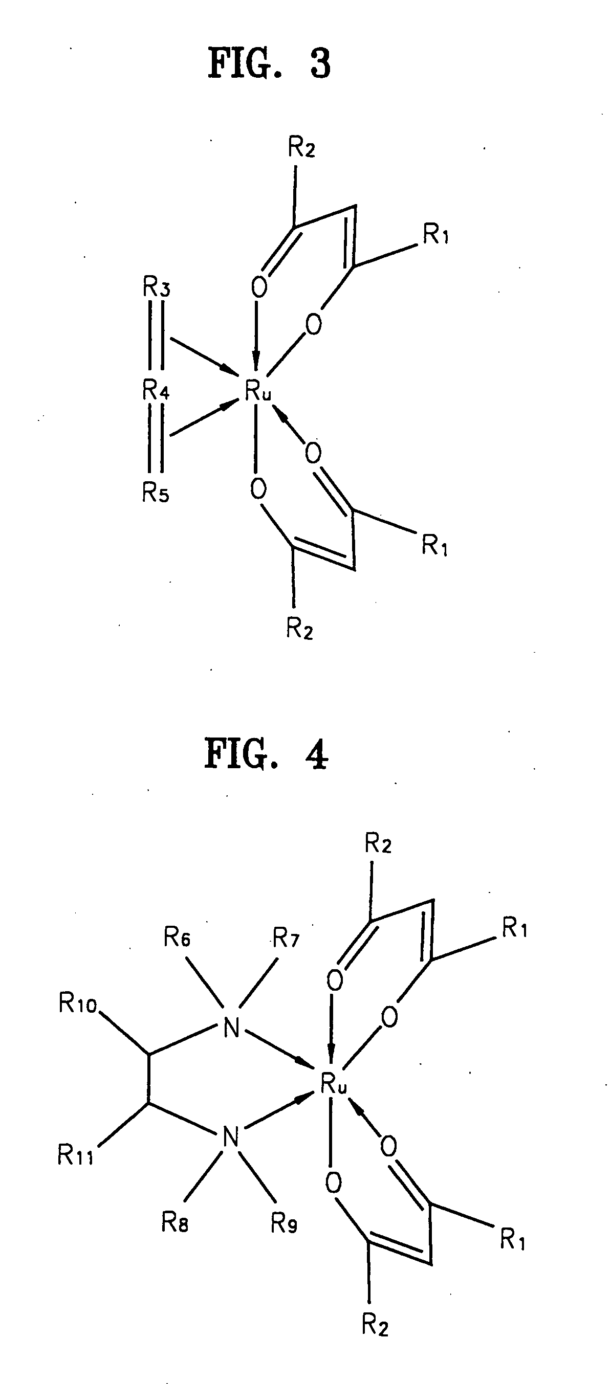
Methods for forming ruthenium films with beta-diketone containing ruthenium complexes and method for manufacturing metal-insulator-metal capacitor using the same
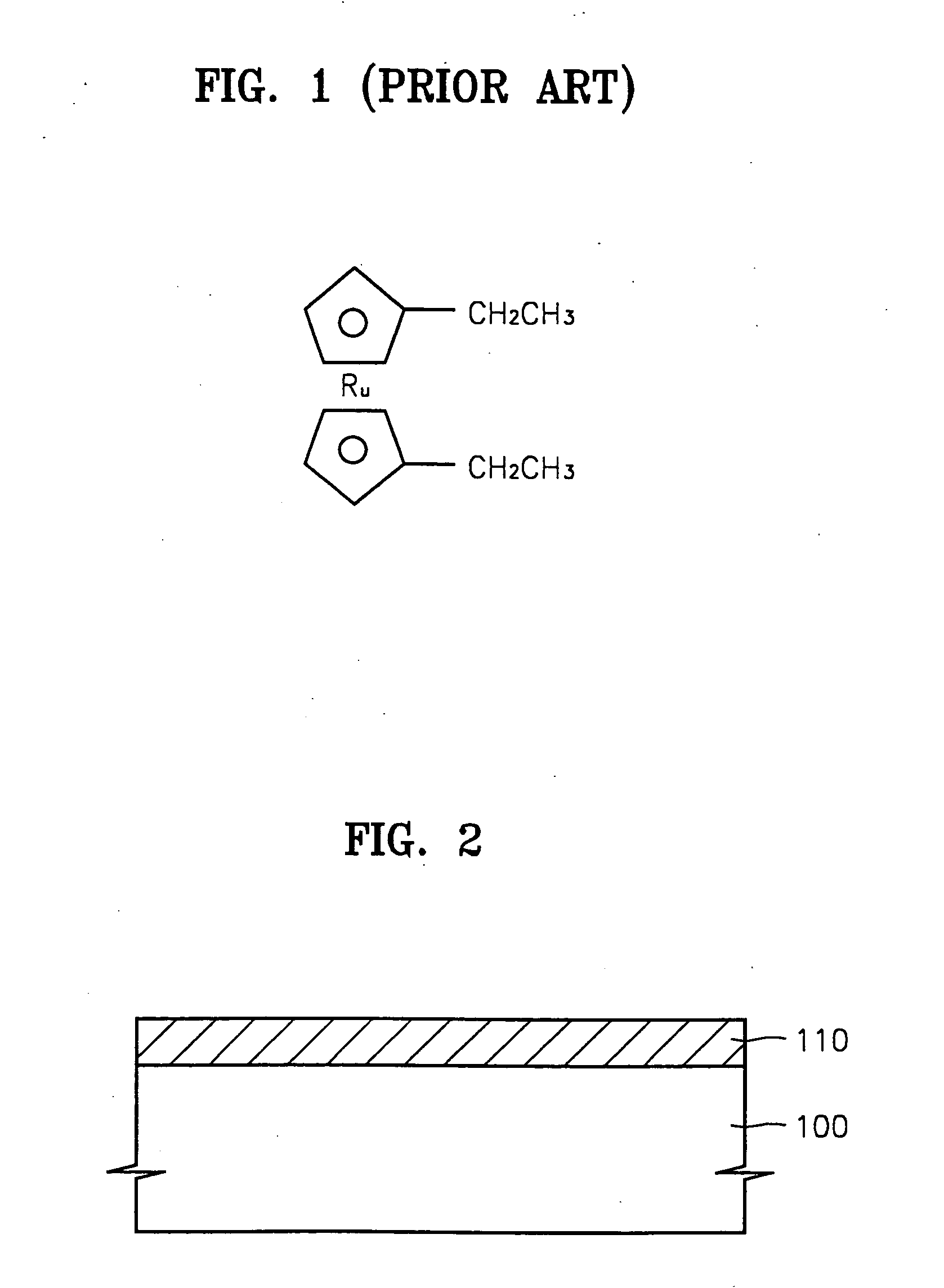
a technology of beta-diketone and ruthenium complex, which is applied in the direction of coatings, solid-state devices, chemical vapor deposition coatings, etc., can solve the problems of difficult nucleation of bis(ethylcyclopentadienyl)ruthenium, high nucleation rate per unit area, and high cost of ruthenium film production. , to achieve the effect of high adhesion of ruthenium film to a lower layer
- Summary
- Abstract
- Description
- Claims
- Application Information
AI Technical Summary
Benefits of technology
Problems solved by technology
Method used
Image

Examples
Embodiment Construction
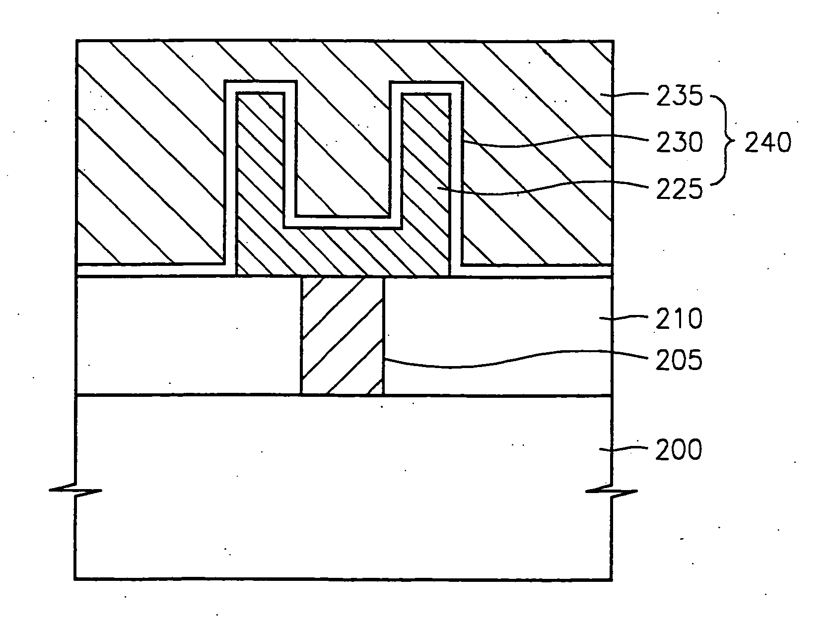
[0044] Hereinafter, exemplary embodiments of the present invention will be described with reference to the accompanying drawings. However, the present invention is not limited to these embodiments and various modifications can be carried out. The embodiments of the present invention are provided to assist ordinary persons skilled in the art to more clearly understand the present invention. In this regard, each constitutional element on drawings is graphically expressed for proper understanding. The same numerals are used for the corresponding constitutional elements in drawings. As used herein, the expression “a first layer is formed ‘on’ a second layer or a semiconductor substrate” includes the case where the first layer indirectly contacts with the second layer due to a third layer between the first layer and the second layer, in addition to direct contact of the first layer and the second layer.
[0045] Referring to FIG. 2, first, a semiconductor substrate 100 is placed in a chamb...
PUM
| Property | Measurement | Unit |
|---|---|---|
| temperature | aaaaa | aaaaa |
| pressure | aaaaa | aaaaa |
| pressure | aaaaa | aaaaa |
Abstract
Description
Claims
Application Information