Electrical connection of optoelectronic devices

Inactive Publication Date: 2006-07-13
CAMBRIDGE DISPLAY TECH LTD
View PDF5 Cites 52 Cited by
  • Summary
  • Abstract
  • Description
  • Claims
  • Application Information

AI Technical Summary

Benefits of technology

[0022] In a preferred embodiment said second conductive material partially overlies said first conductive material, such an arrangement enables electrical connections to be more readily made between neighbouring devices. Where the second conductive material only partially overlies the first conductive material removal of the organic optoelectronic material not covered by the second conductive material uncovers regions of the first con

Problems solved by technology

When developing organic electroluminescent devices for use in large area lighting, in addition to the problems which occur in display technology, the skilled person is presented with a range of further problems, in particular how to prepare a large area electroluminescent lig

Method used


Image

  • Electrical connection of optoelectronic devices
  • Electrical connection of optoelectronic devices
  • Electrical connection of optoelectronic devices

Examples


example

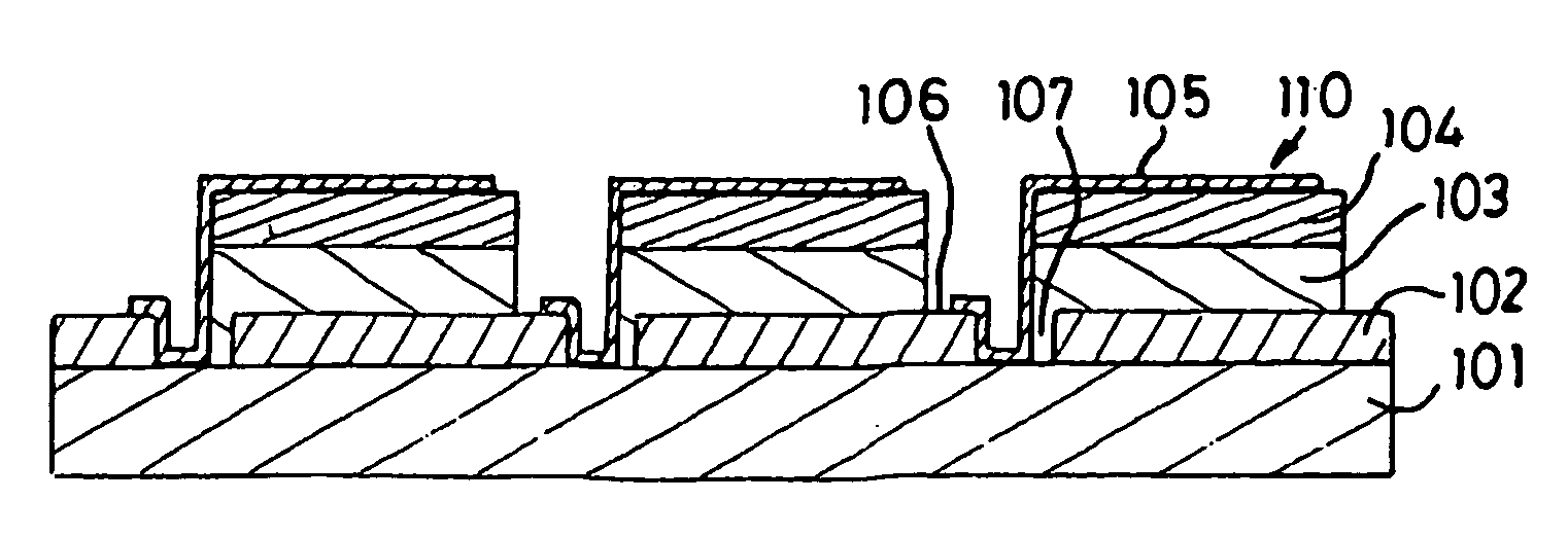
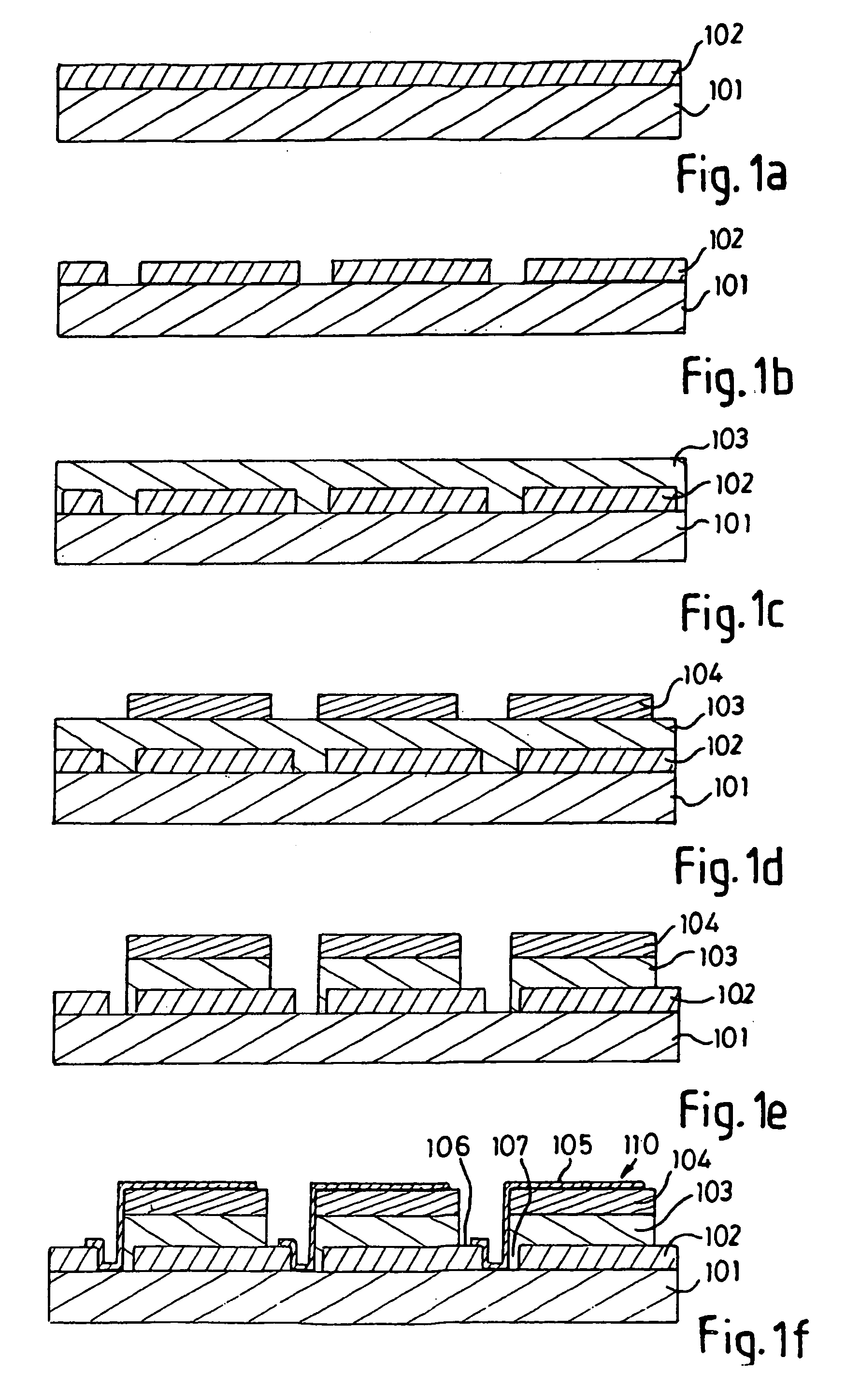
[0068] Series Connected Organic Photovoltaic Devices

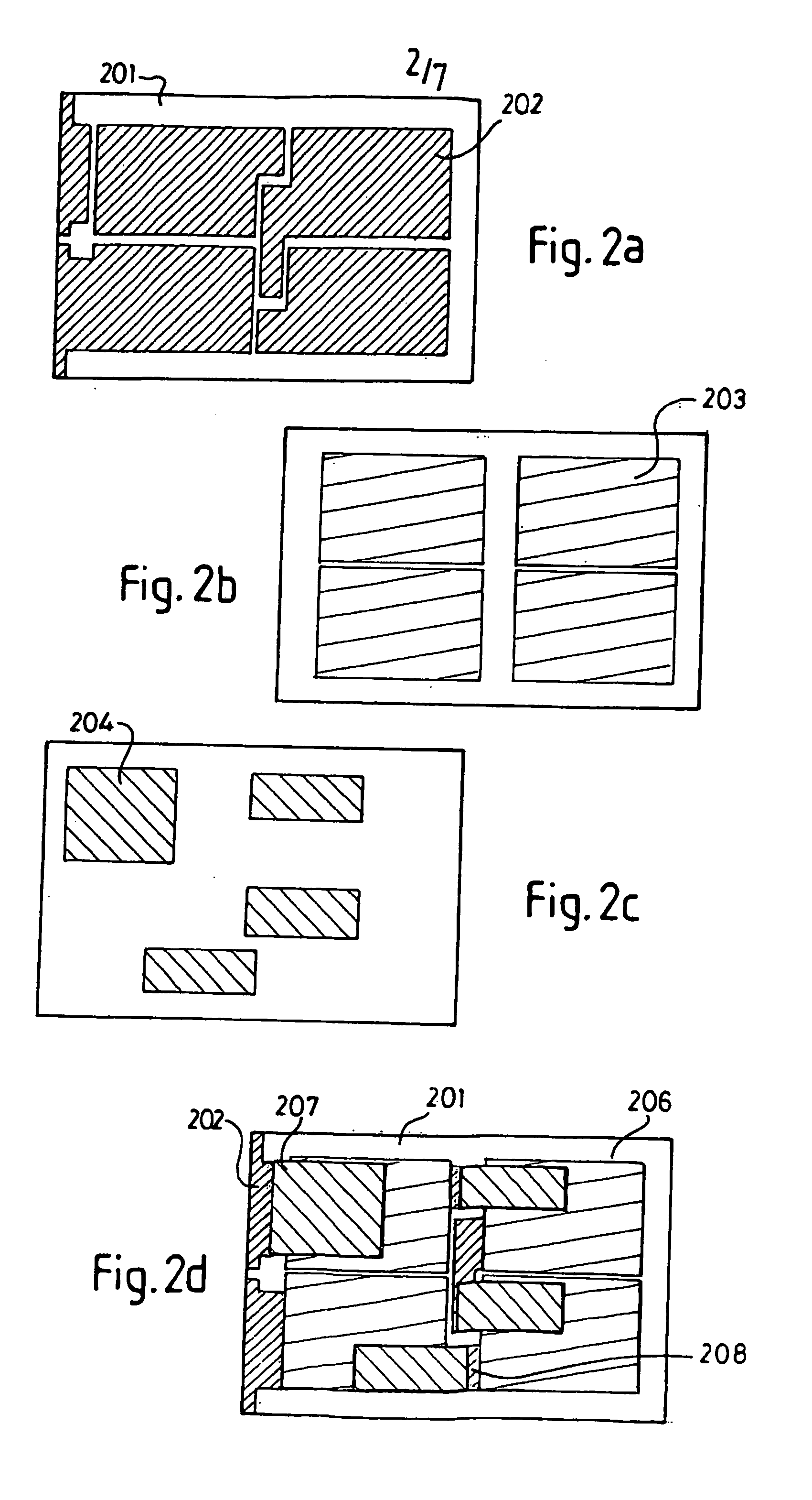
[0069] A substrate patterned with ITO as shown in FIG. 2a) was cleaned in an ultrasonic bath for ten minutes at 60° C., baked for 20 mins at 110° C. and treated with UV / Ozone for 90 s. 10 ml of an aqueous solution of PEDOT:PSS (available from Bayer as Baytron) was spin-coated onto the substrate and the substrate was baked on a hotplate to remove remaining solvent. A layer of PEDOT:PSS having a thickness of 60 nm was deposited. A solution comprising a 1:1 blend of poly(3-hexylthiophene) and poly(2,7-(9,9-di-n-octylfluorene)-(4,7-di-2-thienyl-(benzothiazole)) at a concentration of 18 mg / l in toluene was spin-coated onto the layer of PEDOT:PSS. A layer of polymer blend of thickness 80 nm was deposited. Aluminium cathodes were deposited over the organic layers through a shadow mask. An initial deposition rate of 0.1 nms−1 was maintained to a total thickness of approximately 50 nm, after which the rate was increased to 0.5 nms−1. A tot...


PUM

PropertyMeasurementUnit
Electrical conductoraaaaaaaaaa
Semiconductor propertiesaaaaaaaaaa
Optoelectronic propertiesaaaaaaaaaa

Abstract

A method of preparing a plurality of electrically connected organic optoelectronic devices on a substrate comprising firstly preparing a plurality of organic optoelectronic devices on a substrate, by the steps of providing a patterned layer of a first conductive material over the substrate, providing layer of organic optoelectronic material over the layer of first conductive material and providing a patterned layer of a second conductive material over the layer of organic optoelectronic material, at least partially removing regions of the organic optoelectronic material which are not covered by the patterned layer of second conductive material and secondly providing electrical connections to electrically connect at least two of the plurality of organic optoelectronic devices. The organic optoelectronic devices are suitably organic photovoltaic devices or organic electroluminescent devices.

Description

BACKGROUND OF THE INVENTION [0001] 1. Field of the Invention [0002] The present application is directed to a method of electrical connection of optoelectronic devices such as organic electroluminescent devices and organic photovoltaic devices and to electrically connected devices obtained according to this method. [0003] 2. Brief Description of the Prior Art [0004] The past decade has seen an increasing amount of research into the use of organic materials in optoelectronic devices, examples of such devices include organic electroluminescent devices, as disclosed in WO90 / 13148 and organic photovoltaic devices, as disclosed in U.S. Pat. No. 5,670,791. Both organic electroluminescent devices and organic photovoltaic devices are organic diodes comprising a layer of organic material between two electrodes. Organic electroluminescent devices emit light on the passage of a current between the two electrodes. Organic electroluminescent devices have a wide range of applications in the displa...

Claims


Application Information

Patent Timeline
IPC IPC(8): G02B5/08H01L25/04H01L27/00H01L27/32H01L51/00H01L51/30H01L51/40H01L51/42
CPCB82Y10/00H01L25/047H01L27/301H01L27/3204H01L51/0017H01L51/0036H01L51/0037H01L51/0039H01L51/0043H01L51/4253H01L51/5203H01L2251/308H01L2251/5361H01L2924/0002
Inventor HALLS, JONATHANWILSON, RICHARD
Owner CAMBRIDGE DISPLAY TECH LTD
Why Eureka
Try Eureka