Method for reducing feature line edge roughness

a technology of feature line edge roughness and lithography, applied in the field of lithography manufacturing processes, can solve the problems of copper voiding, difficult to obtain conformal liner coverage, and inability to achieve excessive line edge roughness in the final etched feature, etc., and achieve the effect of reducing line edge roughness

Inactive Publication Date: 2006-07-13
IBM CORP +1
View PDF7 Cites 7 Cited by
  • Summary
  • Abstract
  • Description
  • Claims
  • Application Information

AI Technical Summary

Benefits of technology

[0006] Bearing in mind the problems and deficiencies of the prior art, it is therefore an object of the present invention to provide...

Problems solved by technology

It is undesirable to have excessive line edge roughness in the final etched feature, i.e., along the walls of the feature.
Similarly, in back end of the line (BEOL) processing, it is difficult to obtain conformal liner coverage when the features patterned in the dielectric layer are rough.
Poor liner conformality can cause copper v...

Method used


Image

  • Method for reducing feature line edge roughness
  • Method for reducing feature line edge roughness
  • Method for reducing feature line edge roughness

Examples


Embodiment Construction

(s)

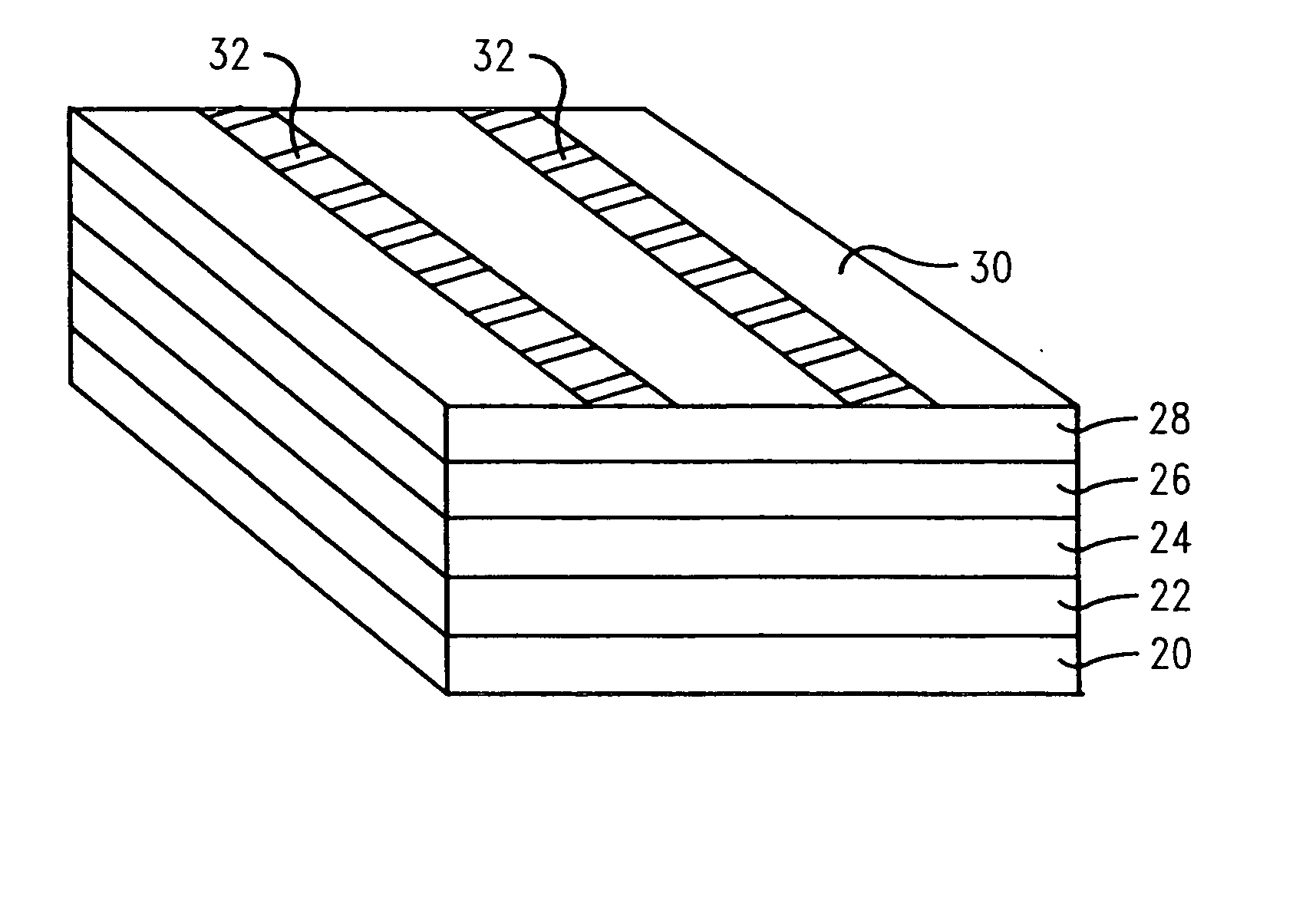
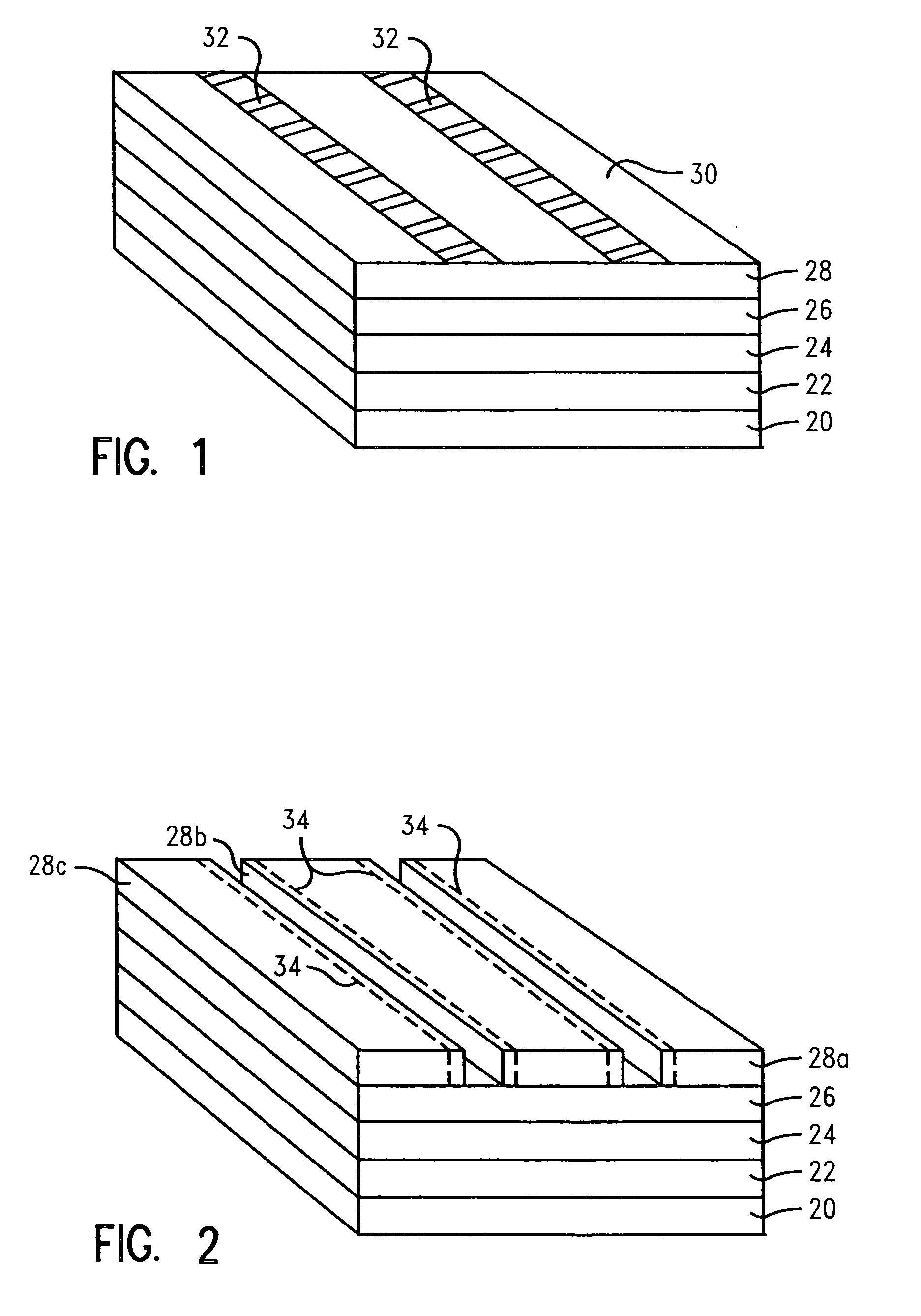
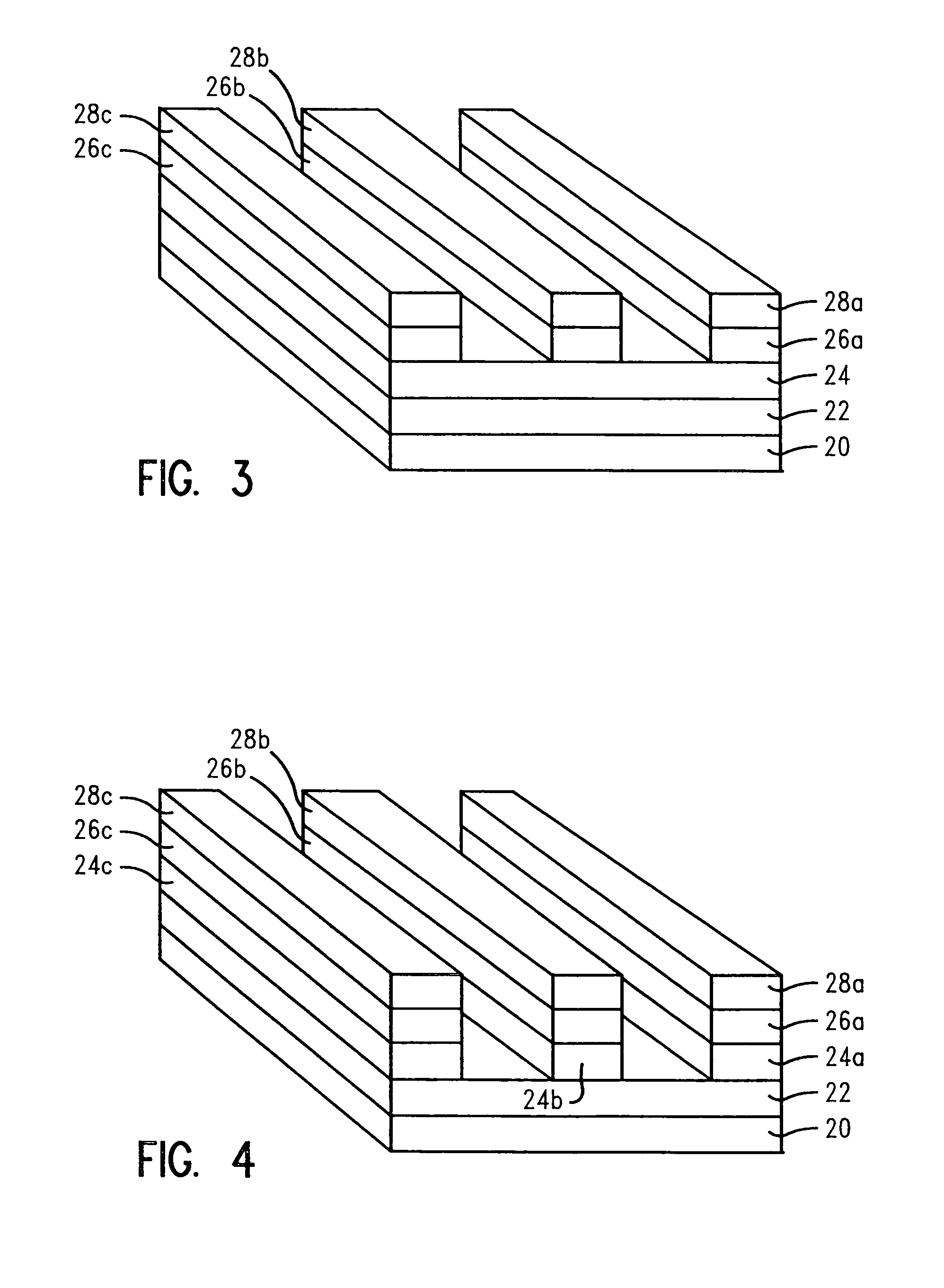
[0024] In describing the preferred embodiment of the present invention, reference will be made herein to FIGS. 1-6 of the drawings in which like numerals refer to like features of the invention.

[0025] The present invention enables the reduction of the line edge roughening phenomenon of the final etch feature by curing the resist layer prior to or during the etch step. During conventional etching processes, high ion bombardment energies can facet and roughen resist features, such that the roughness may transfer into the substrate. The method of the present invention allows the patterning of smoother features without disrupting the existing process flow. The benefits achieved herein are over and above those obtained by optimizing the existing lithography and etching steps.

[0026] The present invention uses resist curing as a method to reduce roughening the resist during etch, which typically then translates to smoother etched profiles in the substrate. Line edge roughness reductio...


PUM


Abstract

A method of patterning a feature in a substrate to reduce edge roughness comprises forming a resist layer overlying a substrate, exposing the resist layer to create an image of a feature, and developing the exposed resist layer to leave a portion of the resist layer that creates the image of the feature. The method then includes treating the exposed resist layer with a plasma to cure the portion of the resist layer creating the feature image. The plasma treatment has an ion bombardment level insufficient to substantially etch the underlying substrate. The method then includes etching the underlying substrate to create the feature.

Description

BACKGROUND OF THE INVENTION [0001] 1. Field of the Invention [0002] The present invention relates generally to manufacturing processes requiring lithography and, more particularly, to the treatment of photoresists suitable for use in the production of microelectronic devices to reduce edge roughness of features produced by plasma etching. [0003] 2. Description of Related Art [0004] Photolithography is used to expose resist layers over substrates used to create microelectronic devices. After the image has been developed, the remaining portion of the resist layer creates the image of the exposed feature, which is then used as a mask to etch underlying substrate materials. It is undesirable to have excessive line edge roughness in the final etched feature, i.e., along the walls of the feature. For example, in front end of the line (FEOL) processing, rough polysilicon gate profiles can affect the doping profiles in the source and drain regions, thereby altering device characteristics. S...

Claims


Application Information

Patent Timeline
IPC IPC(8): G03F7/00
CPCG03F7/40H01L21/0274H01L21/31058H01L21/31144
Inventor MAHOROWALA, ARPAN P.BELL, SCOTT A.MURTHY, S. DAKSHINARASGON, STACY A.YAN, HONGWENYANG, CHIH-YUH
Owner IBM CORP
Why Eureka
Try Eureka