Method for fabricating gaN-based nitride layer

a gallium nitride and gan-based technology, applied in the direction of polycrystalline material growth, crystal growth process, chemically reactive gas growth, etc., can solve the problems of difficult to grow gan-based nitride layer of high quality, gan-based nitride layer has a dislocation density of about 10, and the method has lots of room for improvement, so as to achieve high reliability, good physical properties, and high efficiency

Active Publication Date: 2006-07-13
EPIVALLEY +1
View PDF6 Cites 25 Cited by
  • Summary
  • Abstract
  • Description
  • Claims
  • Application Information

AI Technical Summary

Benefits of technology

[0022] According to the present invention, a non-single crystalline SiC thin layer that has a material different from existing Al(x)Ga(y)In(z)N (0≦x≦1, 0≦y≦1, 0≦z≦1, x+y+z=1) grown by means of a MOCVD method and is grown at a low temperature, is formed on a sapphir

Problems solved by technology

Thus, it is difficult to grow the GaN-based nitride layer of a high quality.
However, although the GaN-based nitride layer is grown by this method, there is a problem in that the GaN-based nitride layer has a dislocation density of about 1010 to 1012/cm2.
However, this method has lots of room for improvement.
Meanwhile, researches on a method for growing silicon carbide (SiC) on a sapphire wafer have rarely been made.
However, this experiment is directed to analysis into the structure of a formed silicon carbide layer, but not to a method

Method used


Image

  • Method for fabricating gaN-based nitride layer
  • Method for fabricating gaN-based nitride layer
  • Method for fabricating gaN-based nitride layer

Examples


first embodiment

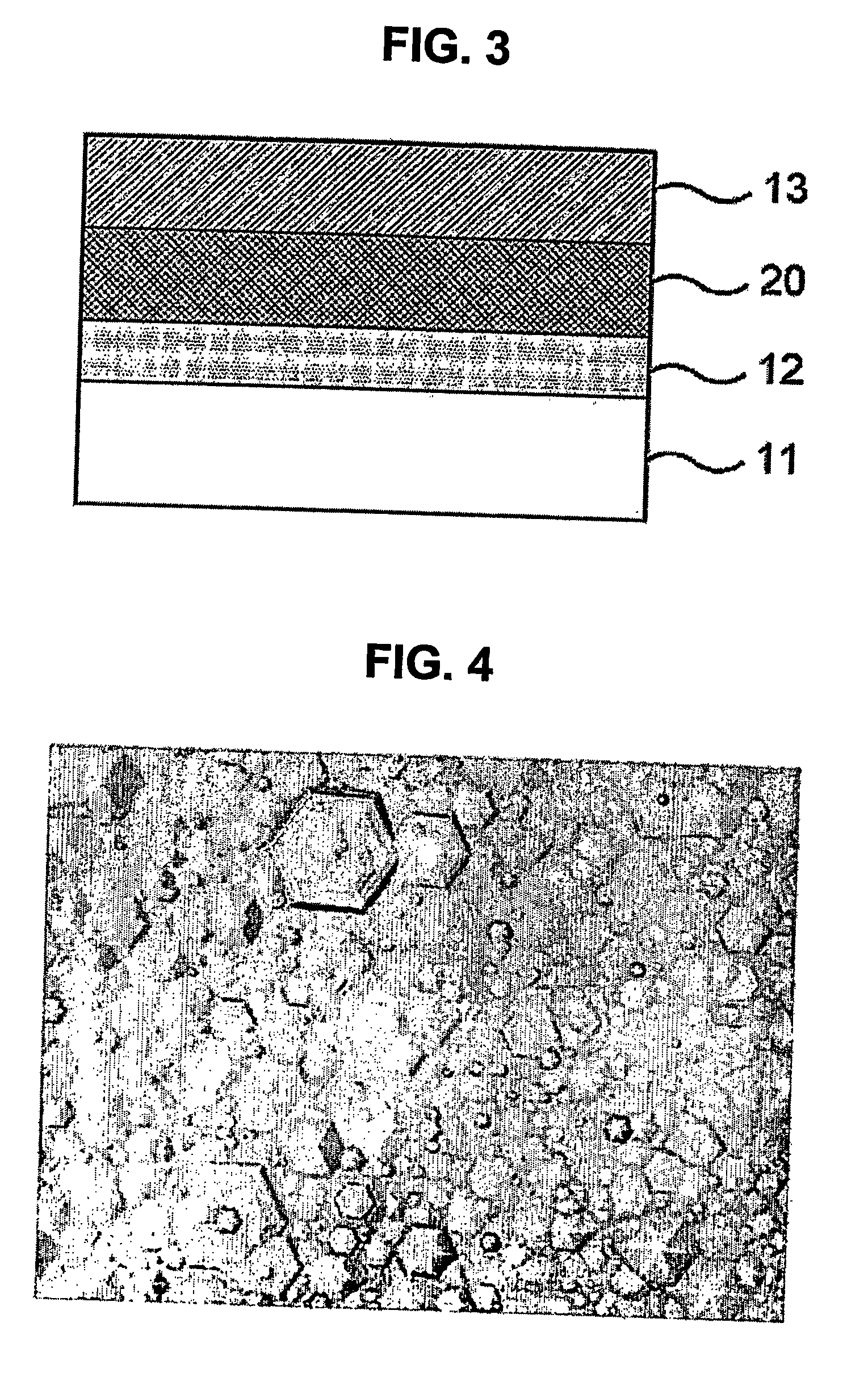
[0042] The structure of the first embodiment according to the present invention is formed by almost the same method as that described in the first comparative example. That is, all process steps and conditions are the same as those of the first comparative example except that in the step of forming the wetting layer 20, the V / III ratio is set to a range between 250 and 300, which is 1 / 20 lower than that of the first comparative example. As such, the structure according to the first embodiment of the present invention is the same as that shown in FIG. 3. Thus, description on it will be omitted in order to avoid redundancy of explanation.

[0043]FIG. 5 is a view showing the shape of the surface of the GaN layer formed by the method of the first embodiment according to the present invention. From FIG. 5, it can be seen that hillocks that can be seen in FIG. 4 almost disappear and a good surface like a mirror is obtained.

[0044] Through the results of the first embodiment, it can be seen...

second embodiment

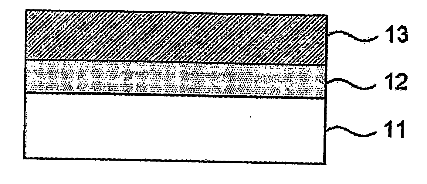
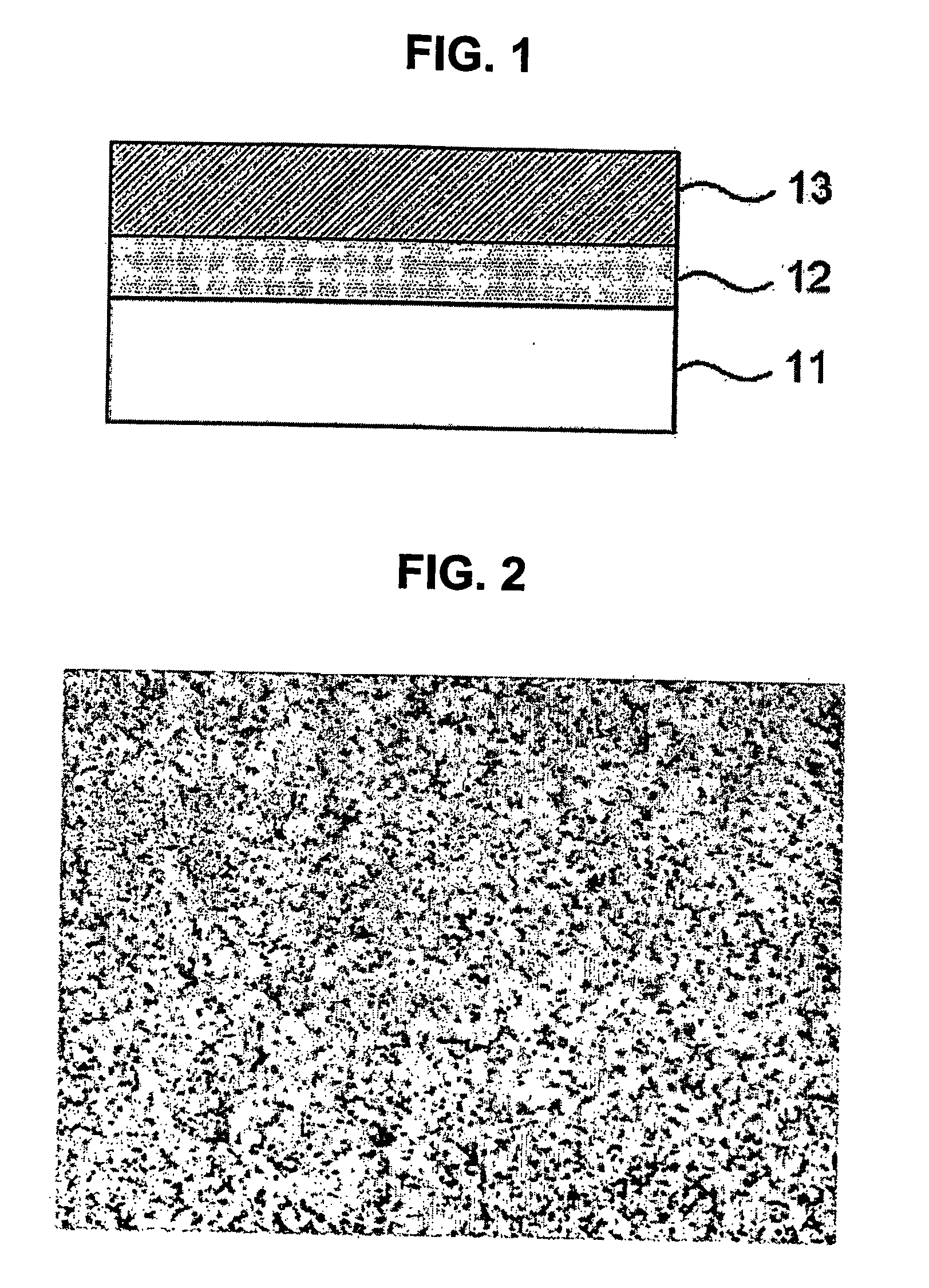
[0047]FIG. 1 is a view showing the second embodiment of the present invention. As shown in FIG. 1, after a SiC buffer layer 12 has been formed on a sapphire substrate 11, a GaN layer 13 is grown immediately on the SiC buffer layer 12 at a high temperature of 900° C. or more.

[0048]FIG. 2 is a view showing the surface of the GaN layer 13 immediately after it has been grown by the method described with reference to FIG. 1. Since the adhesive strength between SiC and GaN is not good, a continuous GaN layer is not formed, but only a discontinuous GaN layer 13 is formed. Therefore, in this case, it is necessary to grow a GaN layer 13 having a thickness enough to overcome such discontinuousness.


PUM


Abstract

The present invention relates to a method for fabricating a gallium nitride(GaN) based nitride layer including a step of forming a wetting layer having of forming a wetting layer having a composition of In(x1)Ga(y1)N (0<x1≦1, 0≦y1<1, x1+y1=1) on the silicon carbide buffer layer, and a step of forming a nitride layer containing gallium and nitrogen on the wetting layer, thereby can implement an opto-electronic device of high efficiency and high reliability.

Description

TECHNICAL FIELD [0001] The present invention relates to a method for fabricating a gallium nitride (GaN) based nitride layer. More particularly, the present invention relates to a method for fabricating a GaN-based nitride layer of a high quality using silicon carbide (SiC) buffer layer and a wetting layer. BACKGROUND ART [0002] In a process of manufacturing semiconductor devices, in order to grow a gallium nitride (GaN) based nitride layer, i.e., a GaN-based nitride layer, substrates composed of, usually, sapphire (Al2O3), silicon carbide (SiC), or the like have mainly been used. They are different from the GaN-based nitride layer in terms of their physical properties such as lattice constant and coefficient of thermal expansion. Thus, it is difficult to grow the GaN-based nitride layer of a high quality. Therefore, lots of schemes for growing the GaN-based nitride layer have been presented continually. [0003] The most representative one includes a method of using a buffer layer. I...

Claims


Application Information

Patent Timeline
IPC IPC(8): H01L21/20H01L21/36H01L31/20C30B25/02C30B29/36C30B29/40H01L33/00
CPCC30B25/02C30B29/36C30B29/403C30B29/406H01L21/0242H01L21/02447H01L21/02458H01L21/02502H01L21/0254H01L21/0262H01L33/007H01L21/20H01L21/34
Inventor JEON, SOO KUNJANG, MOON SIK
Owner EPIVALLEY
Why Eureka
Try Eureka