Optical communication device and optical device

a communication device and optical technology, applied in the field of optical communication devices and optical devices, can solve the problems of increased light insertion loss and limit in the reduction of drive voltage, and achieve the effect of reducing insertion loss

Active Publication Date: 2006-07-20
FUJITSU LTD
View PDF1 Cites 39 Cited by
  • Summary
  • Abstract
  • Description
  • Claims
  • Application Information

AI Technical Summary

Benefits of technology

[0022] In view of the foregoing, an object of the invention is to provide an optical communication device and optical device with low loss and low insertion loss compared with the conventional optical communication device and optical device.
[0028] According to the optical communication device (optical device) of the invention, the output of the first optical modulator is branched by the waveguide coupler, the differential delay is given to each output by the delay connecting section, and the outputs is inputted to the second optical modulator. Namely, the phase relationship between the first light and the second light which are obtained by branching the input light is controlled by the phase control section, the light are coupled to output the third signal light in which the intensity is periodically changed and the fourth signal light whose signal phase is different from that of the third signal light, and the phases are adjusted by the phase adjusting section so that the signal phases of the third signal light and the fourth signal light become equal to each other. Therefore, the modulation is performed by the optical modulating section using the phase adjusted light obtained by the phase adjusting section, so that even the light which is lost as the radiated (leaky) light in the conventional technology can be used for the second optical modulator. As a result, the insertion loss can be reduced compared with the conventional optical modulator.

Problems solved by technology

However, in the RZ optical modulator, because the interaction length is restricted by a chip size, there is a limitation in the reduction of the drive voltage.
However, in the above configuration, a portion where the radiated light is generated is increased by the use of the folding waveguide 114 or by the increase in waveguide length, which generates a problem that the light insertion loss is increased.

Method used


Image

  • Optical communication device and optical device
  • Optical communication device and optical device
  • Optical communication device and optical device

Examples


first modification

(A1) First Modification

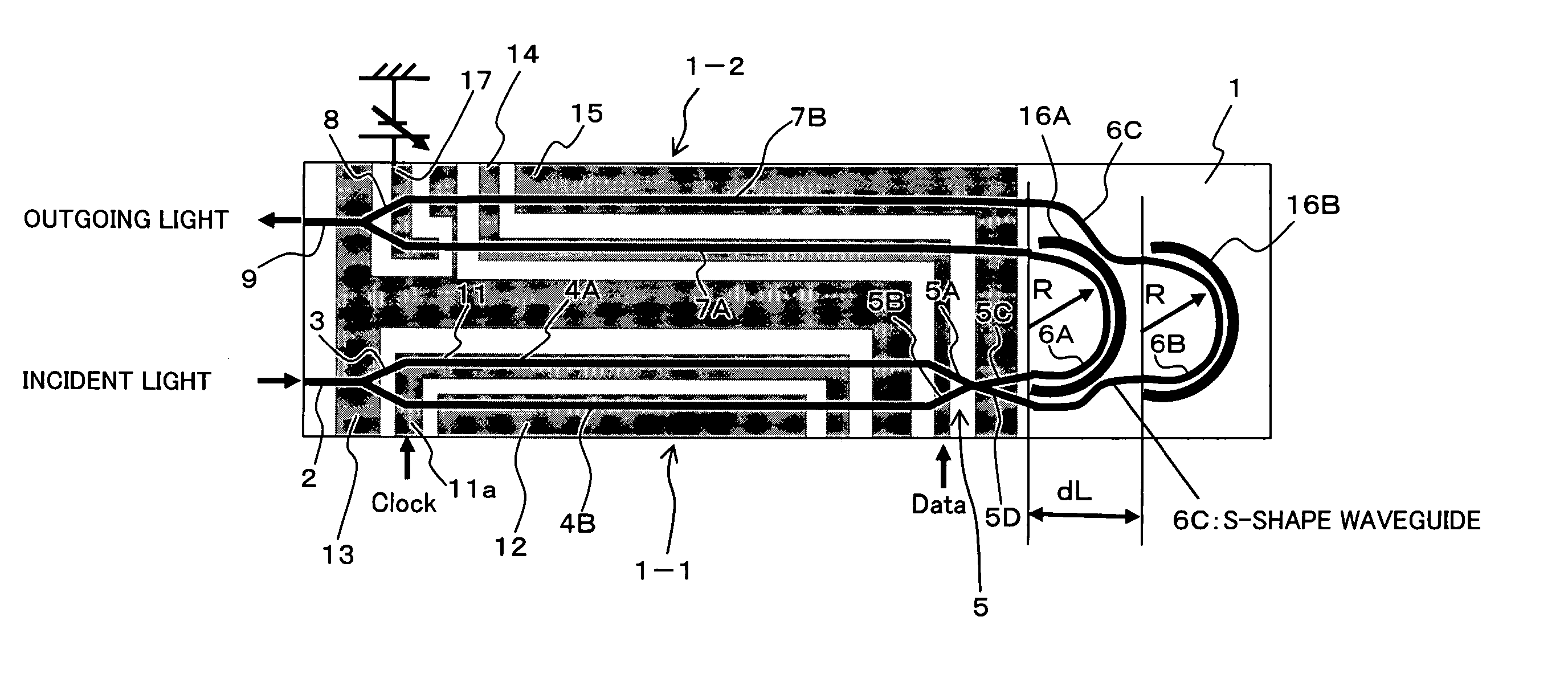
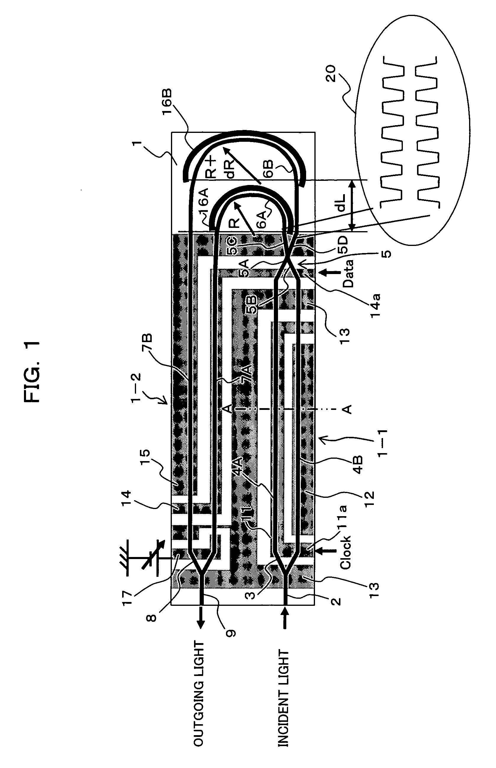
[0071] In the RZ optical modulator shown in FIG. 1, the DC bias electrode 17 is arranged in the Y branching waveguide 8 of the post-stage NRZ modulator 1-2. However, when the DC bias electrode 17 is arranged in the Y branching waveguide 8, it is necessary to shorten the lengths of the electrodes 14 and 15 which overlap the parallel waveguides 7A and 7B, and the drive voltage is increased. Therefore, as shown in FIG. 2, the lengths of the electrodes 14 and 15 can be secured (maintained) as long as possible by arranging the DC bias electrode 17 on the bending waveguide 6B while the DC bias electrode 17 is provided along the bending waveguide 6B. In FIG. 2, the constituent indicated by the same numeral represents the identical or similar constituent described above.

second modification

(A2) Second Modification

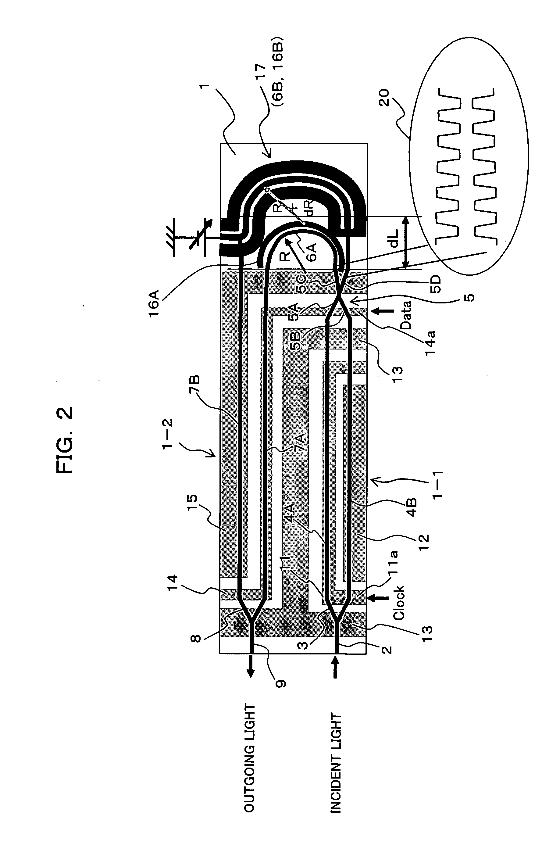
[0072] In the structure shown in FIG. 1, when the difference in curvature radius dR between the bending waveguides 6A and 6B is large, the difference in light intensity between the two light is increased in the post-stage data modulator 1-2, and an extinction ratio of the light output is degraded. In order to prevent the degradation of the extinction ratio of the light output, it is desirable that the difference in curvature radius dR between the bending waveguides 6A and 6B is decreased as much as possible, e.g. the difference in curvature radius dR is set equal to or less than 100 μm. Therefore, as shown in FIG. 5, the curvature radiuses of the two bending waveguides 6A and 6B are set at (R) by inserting an S-shaped waveguide 6C having the larger curvature radius between the input and output portions (indicated by distance dL) of the bending waveguide 6B located on the outer periphery side. Accordingly, the extinction ratio having the same level as for the ...

third modification

(A3) Third Modification

[0073] In the configuration shown in FIG. 1, although the two outputs of the pre-stage clock modulator 1-1 are equal to each other in the output intensity, the chirps are inversed in the polarity. Because the two outputs of the pre-stage clock modulator 1-1 are multiplexed by the 2×2 coupler 5, distortion of the output waveform becomes troublesome in some cases. In the single-drive clock modulator 1-1 shown in FIG. 1, because magnitudes of the electric fields applied to the parallel waveguides 4A and 4B differ from each other as schematically shown in FIG. 7, the chirps inversed in the polarity are generated. FIG. 7 is a sectional view taken on line A-A of FIG. 1.

[0074] In order to avoid the inversed chirps, it is desirable that the amount of chirp generation is zero in the clock modulator 1-1. Therefore, as shown in FIG. 6, it is thought that the clock modulator 1-1 is formed in a dual drive configuration.

[0075] Namely, the signal electrodes 11A and 11B are...


PUM

PropertyMeasurementUnit
interaction lengthaaaaaaaaaa
distanceaaaaaaaaaa
thicknessaaaaaaaaaa

Abstract

An optical communication device includes a substrate which has electro-optical effect; a first optical modulator which has a pair of waveguides formed in the substrate; a second optical modulator which has a pair of waveguides formed in the substrate; a waveguide coupler which is provided in an out put of the first optical modulator, the waveguide coupler being able to couple and branch light propagating through the pair of waveguides of the first optical modulator; and a delay connecting section which gives differential delay to the output branched by the waveguide coupler and inputs the output to the pair of waveguide of the second optical modulator. As a result, the optical communication device and optical device in which insertion loss is reduced compared with the conventional optical modulator can be provided.

Description

CROSS REFERENCE TO RELATED APPLICATIONS [0001] This application is based on and hereby claims priority to Japanese Application No. 2005-7854 filed on Jan. 14, 2005 in Japan, the contents of which are hereby incorporated by reference. BACKGROUND OF THE INVENTION [0002] (1) Field of the Invention [0003] The present invention relates to an optical communication device and an optical device which are used in optical communication, particularly to an RZ optical modulator which is of the optical communication device generating an RZ (Return to Zero) signal. [0004] (2) Description of the Related Art [0005] The optical modulators in which electro-optical crystals such as a LiNbO3 (lithium niobate (LN) ) crystal substrate and a LiTaO2 (lithium tantalate) crystal substrate are used can be cited as typical representatives of the optical communication device. For production of the optical communication device, an optical waveguide is formed by depositing a metal film on a part of the crystal su...

Claims


Application Information

Patent Timeline
Patent Type & Authority Applications(United States)
IPC IPC(8): G02F1/035
CPCG02F1/035G02F1/0356G02F2201/16G02F2201/20
Inventor SUGIYAMA, MASAKI
Owner FUJITSU LTD
Why Eureka
Try Eureka