
Gate stack engineering by electrochemical processing utilizing through-gate-dielectric current flow

a dielectric current and gate stack technology, applied in the field of electrochemical processing, can solve the problems of no chemical modification, self-limiting formation of passive native oxides on substrates, etc., and achieve the effect of less resistan

Active Publication Date: 2006-07-27
GLOBALFOUNDRIES US INC
View PDF17 Cites 69 Cited by
  • Summary
  • Abstract
  • Description
  • Claims
  • Application Information

AI Technical Summary

Benefits of technology

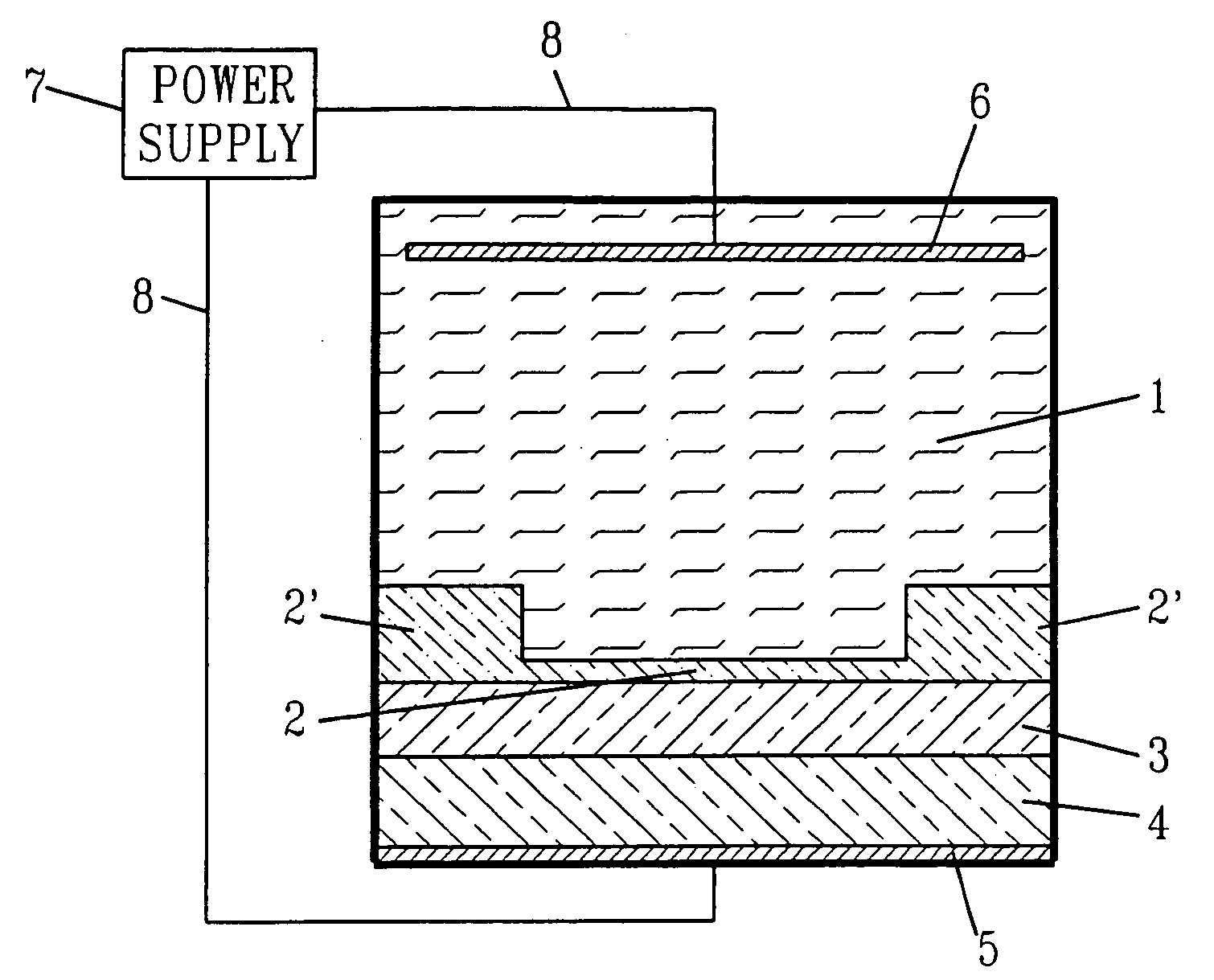
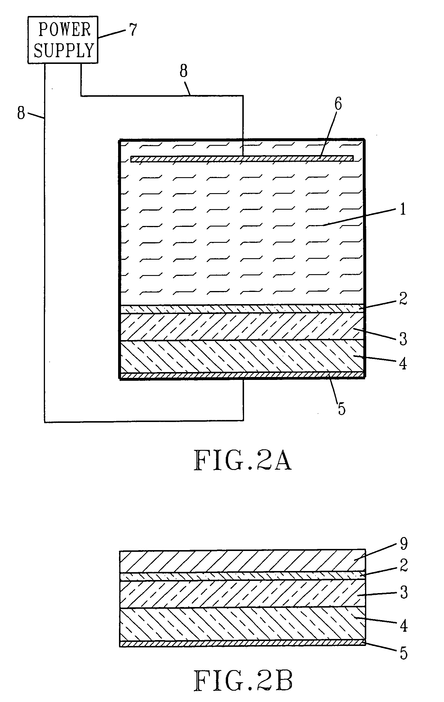
[0021] In a fourth aspect of the invention, electrochemical methods are provided for electroetching of thin dielectrics and / or electrodeposition of additional insulator films onto the thin dielectric by through-dielectric current flow. The electroetching and / or electrodeposition may be spatially selective or nonselective.
[0022] A fifth aspect of this invention provides structures made by the methods of this invention. In particular, the invention provides FET devices containing metal gates formed by electrodeposition directly onto the gate dielectric.

Problems solved by technology

Formation of a passive native oxide on a substrate tends to be self-limiting, since the process stops when the electrochemically formed oxide is thick enough to prevent current flow.
However, no chemical modifications (i.e., introduction of new elements not already in the dielectric) would be expected with the non-reactive solution chemistry employed (dilute aqueous HF), and the treatment is directed toward modifying the bulk of the dielectric, rather than its surface.

Method used


Image

  • Gate stack engineering by electrochemical processing utilizing through-gate-dielectric current flow
  • Gate stack engineering by electrochemical processing utilizing through-gate-dielectric current flow
  • Gate stack engineering by electrochemical processing utilizing through-gate-dielectric current flow

Examples


Embodiment Construction

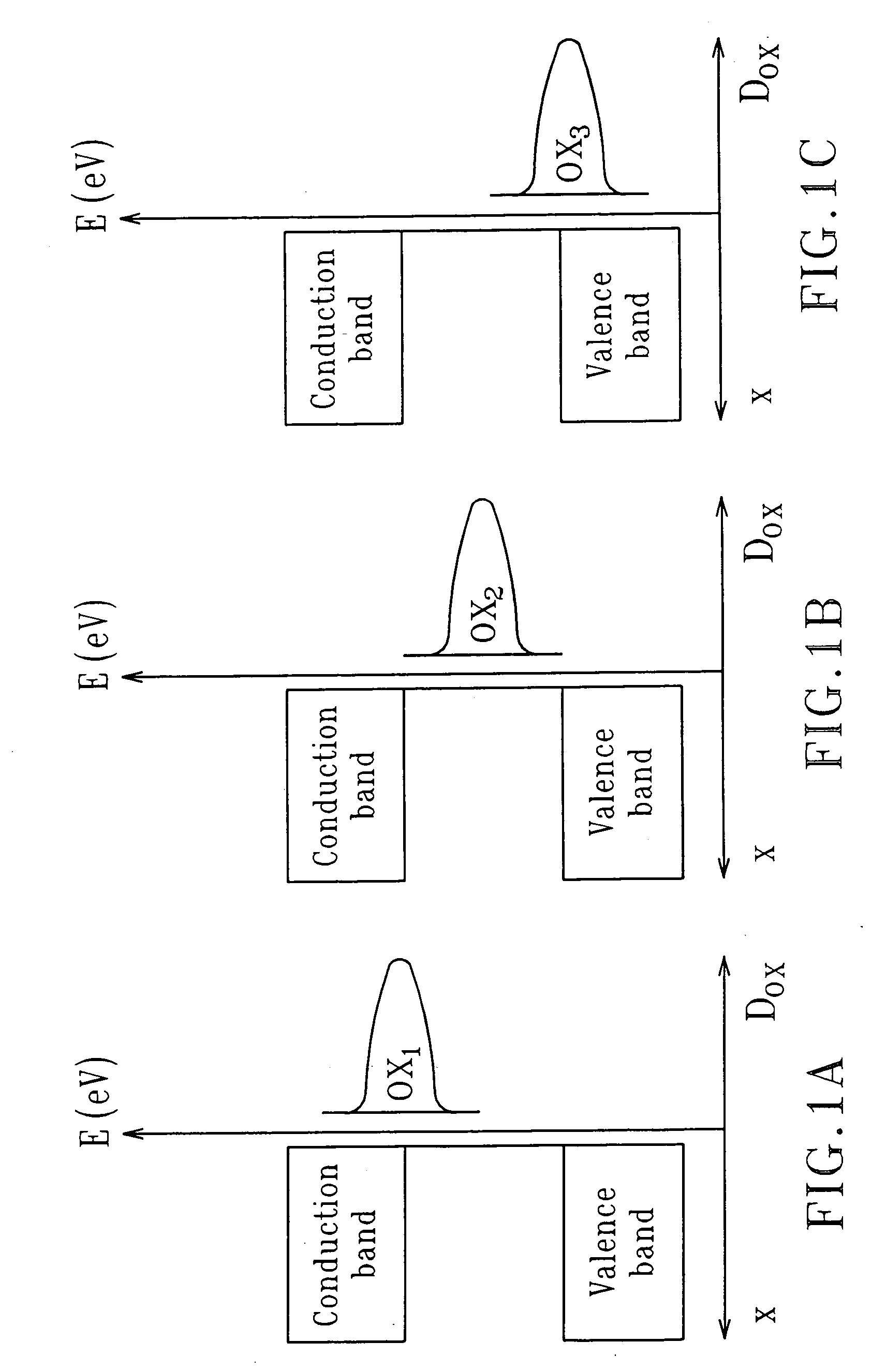
[0043] Electrochemical processing of insulating materials or insulators can potentially occur where the insulator, typically a thin oxide coating on a metal or semiconductor, has some conductance to electrical current. For thin coatings, electron tunneling can be a primary mechanism for dielectric conductivity or current leakage which can be employed for electrochemical processing. Defects can also provide many electron states in the band gap of an insulator, and for a high density of gap states, these can also form a possible pathway for the electrical current. Conductance can also be provided by transport of charges directly through the valence or conduction band of the oxide. The latter case becomes important when working with semiconducting oxides such as TiO2, ZnO and Ta2O5, as well as any n-type wide band-gap semiconductor.

[0044] Since electroplating generally occurs in solution, the possibility of an electrochemical current at the oxide / electrolyte interface depends on sever...


PUM

PropertyMeasurementUnit
thicknessaaaaaaaaaa
thicknessaaaaaaaaaa
current densityaaaaaaaaaa

Abstract

A method is provided for electroplating a gate metal or other conducting or semiconducting material directly on a dielectric such as a gate dielectric. The method involves selecting a substrate, dielectric layer, and electrolyte solution or melt, wherein the combination of the substrate, dielectric layer, and electrolyte solution or melt allow an electrochemical current to be passed from the substrate through the dielectric layer into the electrolyte solution or melt. Methods are also provided for electrochemical modification of dielectrics utilizing through-dielectric current flow.

Description

FIELD OF THE INVENTION [0001] This invention relates to electroplating on a gate dielectric to form a gate electrode. In general, the invention pertains to electrochemical processes such as electrodeposition, electroetching, and / or electromodification, implemented in such a manner as to allow current flow through at least one dielectric layer. BACKGROUND OF THE INVENTION [0002] Electrochemical processing of oxides on metals and semiconductors is well-known in the art of passive oxide formation and electroetching. Formation of a passive native oxide on a substrate tends to be self-limiting, since the process stops when the electrochemically formed oxide is thick enough to prevent current flow. By correct control of the process conditions, good coatings can be obtained. In this regard, see, for example, U.S. Published Application No. 2002 / 0104761 A1, to Birss et al., the entire disclosure of which is incorporated herein by reference. [0003] The formation of reliable SiO2 gate oxides o...

Claims


Application Information

Patent Timeline
Patent Type & Authority Applications(United States)
IPC IPC(8): H01L21/20
CPCC25D3/50C25D5/02C25D5/024C25D5/54C25D9/04C25F3/14H01L21/28079H01L21/28114H01L21/2885H01L21/76885H01L29/513H01L29/517H01L29/78648C25D7/123C25D5/56
Inventor VEREECKEN, PHILIPPE M.BASKER, VEERARAGHAVAN S.CABRAL, CYRIL JR.COOPER, EMANUEL I.DELIGIANNI, HARIKLIAFRANK, MARTIN M.JAMMY, RAJARAOPARUCHURI, VAMSI KRISHNASAENGER, KATHERINE L.SHAO, XIAOYAN
Owner GLOBALFOUNDRIES US INC
Learn More