Programmable matrix array with chalcogenide material

a chalcogenide material and matrix array technology, applied in semiconductor devices, digital storage, instruments, etc., can solve the problems of increasing the tooling cost and time delay of the first article product, increasing the voltage margin, increasing the drain of the battery, etc., to reduce the number of programmable connections, the effect of reducing the number of leakage and reducing the impedan

Active Publication Date: 2006-08-03
OVONYX MEMORY TECH LLC
View PDF1 Cites 60 Cited by
  • Summary
  • Abstract
  • Description
  • Claims
  • Application Information

AI Technical Summary

Benefits of technology

[0038] The programmable connection may be tested by programming the phase-change material to the set state and then to the reset state. It is noted, that only those programmable connections which may potentially be CLOSED (initially or later) would need the breakdown layer's penetrated at factory or at initial customer test. For example, if a customer knows that certain cross-points in a general purpose FPLA will probably not be used in a certain application, the breakdown layers of the corresponding programmable connections need not be penetrated. Since the breakdown layer causes the programmable connection to have higher impedance until penetrated, the leakage is thereby reduced while retaining general flexibility at each X-Y interconnection to program it later, if needed. The dielectric, if viewed as an anti-fuse, is thereby made reversible in the field.
[0039] Permanently wired interconnects may also be used for other logic connections in order to reduce the number of programmable connections, thereby further reducing leakage as well as test requirements. Alternately, an SRAM programmable connection like those shown in FIG. 1 (or one or more other existing alternatives familiar to those reasonably skilled in the art) may be wired in parallel with or used on the same chip with the phase-change programmable connections disclosed herein, such as where faster programming is necessary.

Problems solved by technology

This approach may be characterized by good layout efficiency and performance, but higher tooling costs and time delay to first article product, since custom masks and layout are used for each different customer product and these may need to be generated and applied to silicon before the customer specific product is completed.
That is, any resistor between the lines bleeds current and increases battery drain, while decreasing the voltage margin.
The power drained off by the cross-points intended to be OPEN is a larger problem in larger logic arrays with more X-Y interconnects, and hence more cross-points.
Upon power-on restart, the logic interconnect pattern may be reloaded into the configuration memory elements controlling the interconnect between logic gates and other functions, at the expense of delayed restart.
This full mux approach may provide a lower resistance but it may be at the expense of greater capacitance and increased chip area for each matrix switch.
However, such an approach increases process complexity.
Further, both the SRAM or the non-volatile memory alternative may require considerable area in the base silicon to control the interconnect transistor.
Once programmed to a lower resistance state, an anti-fuse cannot be readily reversed.
Accordingly, testing prior to shipping or in the field (at the OEM manufacturer or by the customer) may be difficult, since reversing a programmed anti-fuse may be impractical.
Also, subsequent changes in the field, such as by remote connection via modem or internet, may not be possible that could reduce repair and upgrade costs since the anti-fuse, once punctured into a low resistance state, may not be reversible (other than by impractically high current, which may adversely affect reliability).
However, while such an option is possible with SRAM or its non-volatile re-programmable equivalent (such as Flash, EEPROM, or FeRam), such an option may not be possible with an anti-fuse based approach.
Instead, the part must instead be removed and replaced, perhaps at considerable expense to the manufacturer and inconvenience to the customer.
Further, due to the limitations of programming irreversible links, such as anti-fuse based FPGA, in only one direction (to be a short), testing of the arrays intended for use by the customer may be done only indirectly, such as by programming spare (unused) but representative anti-fuses along side the main array of interconnect fuses before a part is shipped.
However, actual programming of (untested) links by the customer may be unsuccessful, since the links or cross-points actually used may be defective since they were untested before being shipped or used.
Cross-points found unprogrammable may require return of the unit to the factory or even replacement in the final equipment, if personalization is done after assembly.
Each of these discards may be at successively higher cost and require an undesirable manufacturing and field use flow which is incompatible with a more preferred zero-defect manufacturing and use.
Further, the non-SRAM based approaches may add processing steps beyond those of making the logic to be interconnected, and those extras processing steps may excessively raise cost.

Method used


Image

  • Programmable matrix array with chalcogenide material
  • Programmable matrix array with chalcogenide material
  • Programmable matrix array with chalcogenide material

Examples


Embodiment Construction

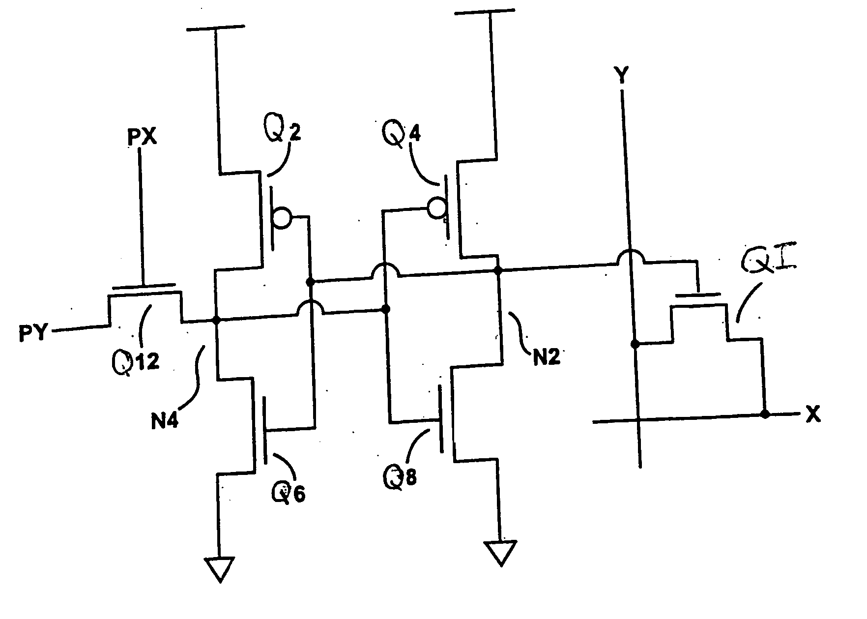
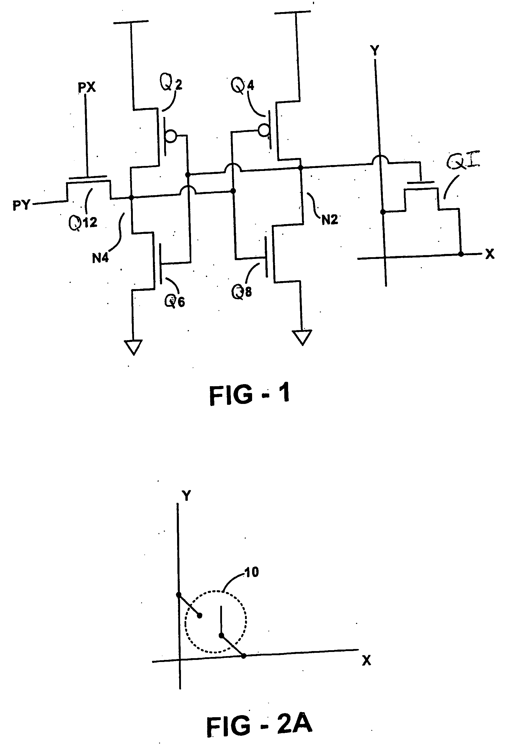
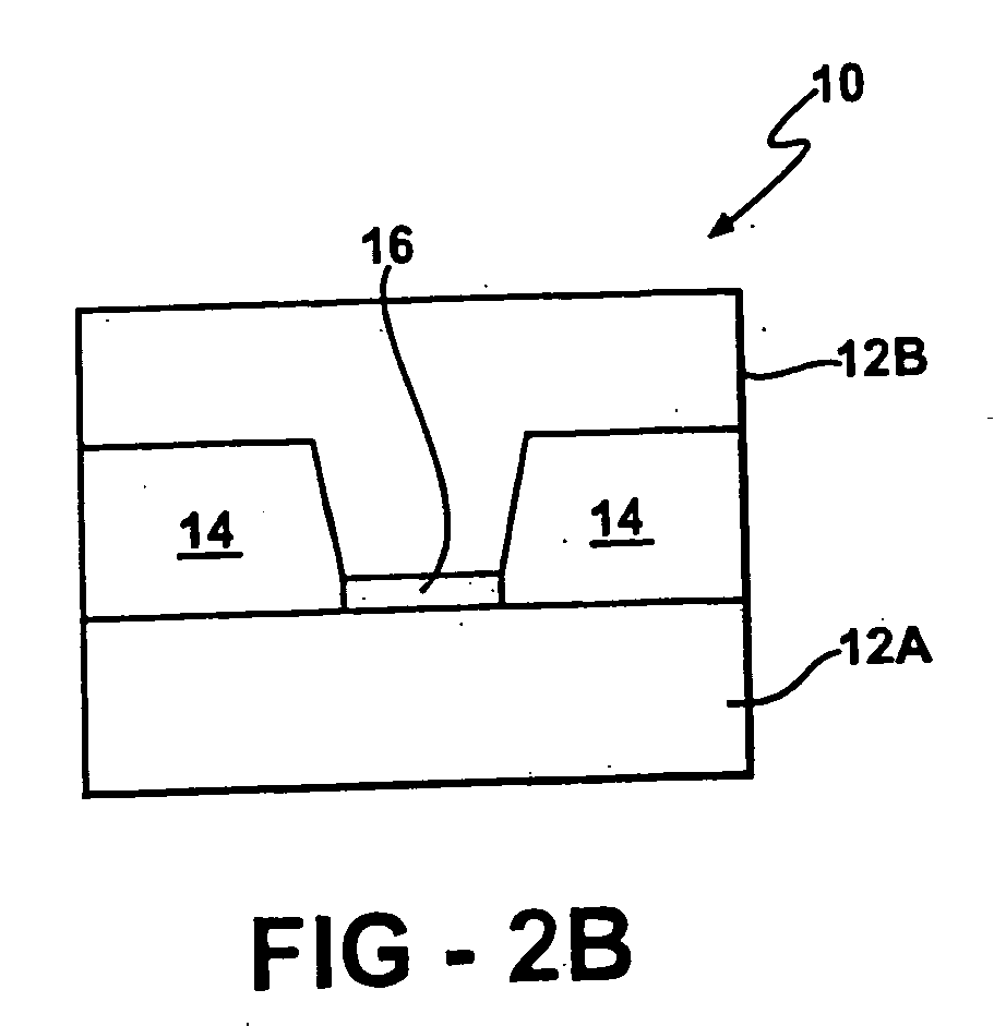
[0143]FIG. 3 shows an embodiment of an electrically programmable matrix array 100 of the present invention. The programmable matrix array 100 may be used in a programmable logic device. The matrix array includes a first set of conductive lines X1 through X4 which are also referred to as X lines. The X lines may be row lines or word lines. The matrix array includes a second set of conductive lines Y1 through Y4 which are also referred to as Y lines. The Y lines may be column lines or bit lines. In the example shown (not meant to be limiting), there are four X lines and four Y lines. However, more generally, there may be one or more X lines, and there may be one or more Y lines. In one or more embodiments there may be a plurality of X lines and a plurality of Y lines. In one or more embodiments of the invention, the X lines and the Y lines may be address lines. In one or more embodiments of the invention, it may even be possible that there be more or fewer X lines, and even one or zer...


PUM


Abstract

A chalcongenide material is proposed for programming the cross-connect transistor coupling interconnect lines of an electrically programmable matrix array. Leakage may be reduced by optionally placing a thin insulating breakdown layer in series with the select device or a phase change material. The matrix array may be used in a programmable logic device.

Description

RELATED APPLICATION INFORMATION [0001] This application is a continuation-in-part of U.S. patent application Ser. No. 10 / 459,632, filed on Jun. 11, 2003. This application is also a continuation-in-part of U.S. patent application Ser. No. 11 / 032,792, filed on Jan. 11, 2005. This application is also a continuation-in-part of U.S. patent application Ser. No. 11 / 158,619, filed on Jun. 21, 2005. U.S. patent application Ser. No. 10 / 459,632 is hereby incorporated by reference herein. U.S. patent application Ser. No. 11 / 032,792 is hereby incorporated by reference herein. U.S. patent application Ser. No. 11 / 158,619 is hereby incorporated by reference herein.FIELD OF THE INVENTION [0002] The present invention generally relates to programmable integrated circuit devices, and more particularly to a programmable matrix array with programmable connections determined by a phase-change material driving a cross-point coupled transistor. BACKGROUND OF THE INVENTION [0003] Generally, phase-change mate...

Claims


Application Information

Patent Timeline
Patent Type & Authority Applications(United States)
IPC IPC(8): G11C11/00
CPCG11C13/0004G11C13/003G11C2213/72G11C2213/75G11C2213/76G11C2213/79H01L27/2427H10B63/24
Inventor LOWREY, TYLERPARKINSON, WARDWICKER, GUY
Owner OVONYX MEMORY TECH LLC
Why Eureka
Try Eureka