Wide wavelength range silicon electroluminescence device

a silicon electroluminescence and wide wavelength range technology, applied in the field of integrated circuit (ic) fabrication, can solve the problems of limiting the use of practical el devices, reducing the peak height (intensity) decay, etc., and achieves the reduction of defects in si-rich silicon dioxide materials, limiting their use in practical el, and increasing the wavelength range

Inactive Publication Date: 2006-08-17
SHARP LAB OF AMERICA INC
View PDF5 Cites 28 Cited by
  • Summary
  • Abstract
  • Description
  • Claims
  • Application Information

AI Technical Summary

Benefits of technology

[0011] The present invention relates to the fabrication of EL and LED devices. The invention describes a method for controlling the grain size of nano crystal Si, and reducing the defects in Si-rich silicon dioxide materials for EL and LED device applications, using DC sputtering, thermal oxidation annealing, and plasma oxidation processes. Conventionally, the photoluminescence PL peak of SRSO materials is located in the wavelength range of 590 nm - 750 nm, and these SRSO materials exhibit a stability problem, wh...

Problems solved by technology

Conventionally, the photoluminescence PL peak of SRSO materials is located in the wavelength range of 590 nm - 750 nm, and these SRSO materials ...

Method used


Image

  • Wide wavelength range silicon electroluminescence device
  • Wide wavelength range silicon electroluminescence device
  • Wide wavelength range silicon electroluminescence device

Examples


Embodiment Construction

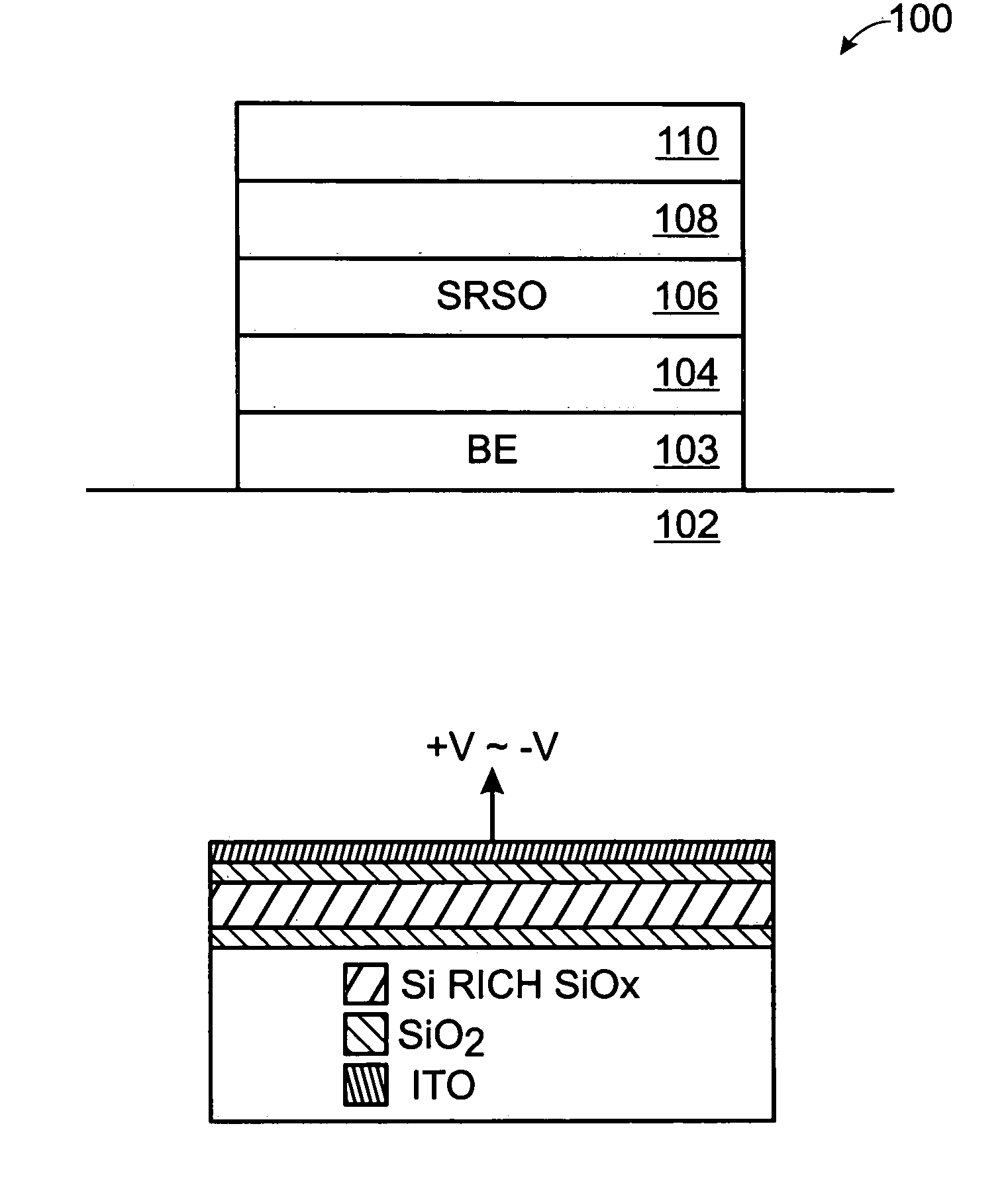
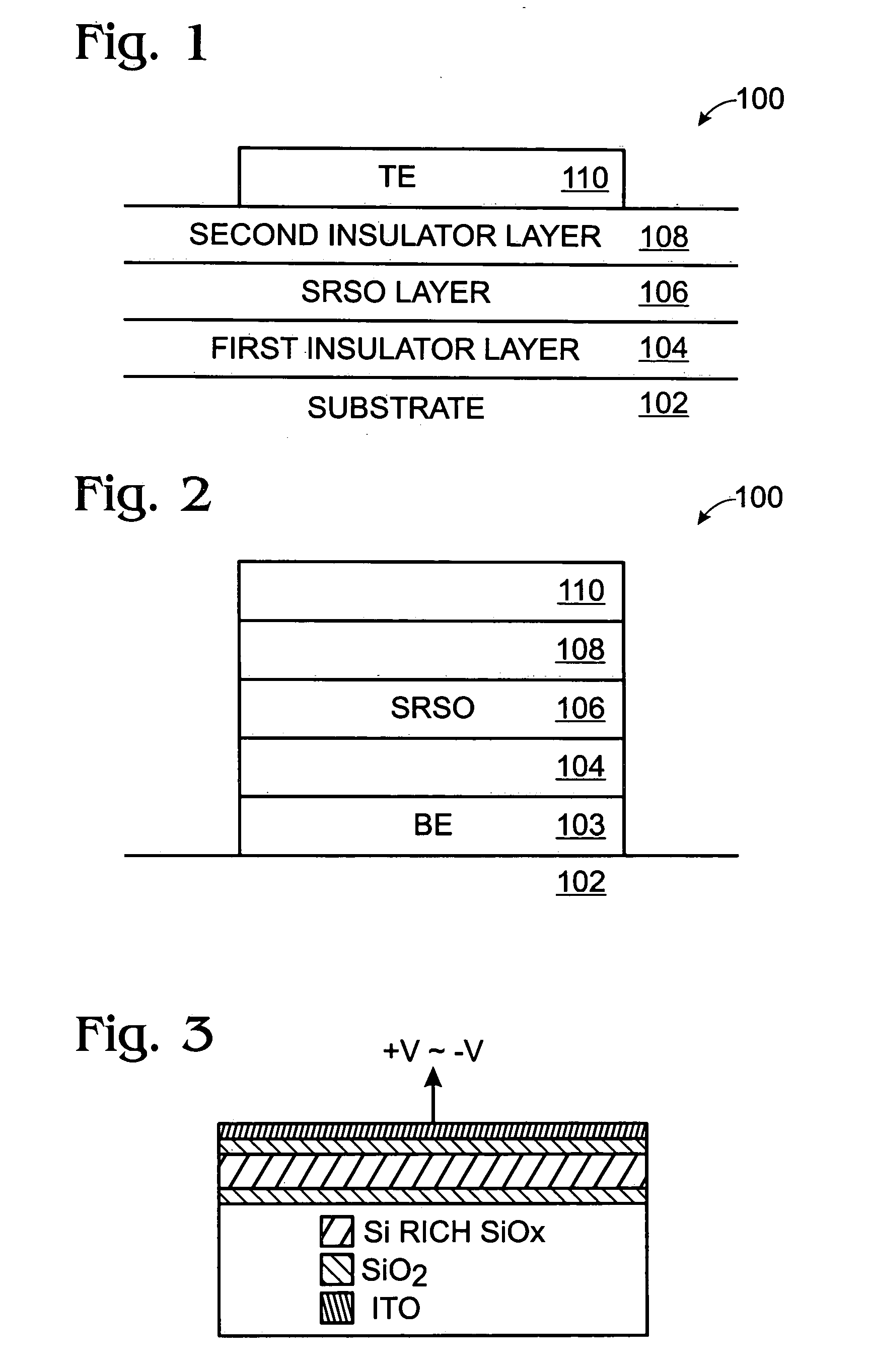
[0026]FIG. 1 is a partial cross-sectional view of a short-wavelength silicon (Si) electroluminescence (EL) device. The device 100 comprises a substrate 102, a first insulator layer 104 overlying the substrate 102, and a silicon-rich silicon oxide (SRSO) layer 106 overlying the first insulator layer 104. The SRSO layer 106 is embedded with nanocrystalline Si having a size in the range of 0.5 to 5 nm. Typically, the SRSO layer 106 has a Si richness in the range of 5 to 40%. A second insulator layer 108 overlies the SRSO layer 106 , and a top electrode 110 (TE) overlies the second insulator layer 108 .

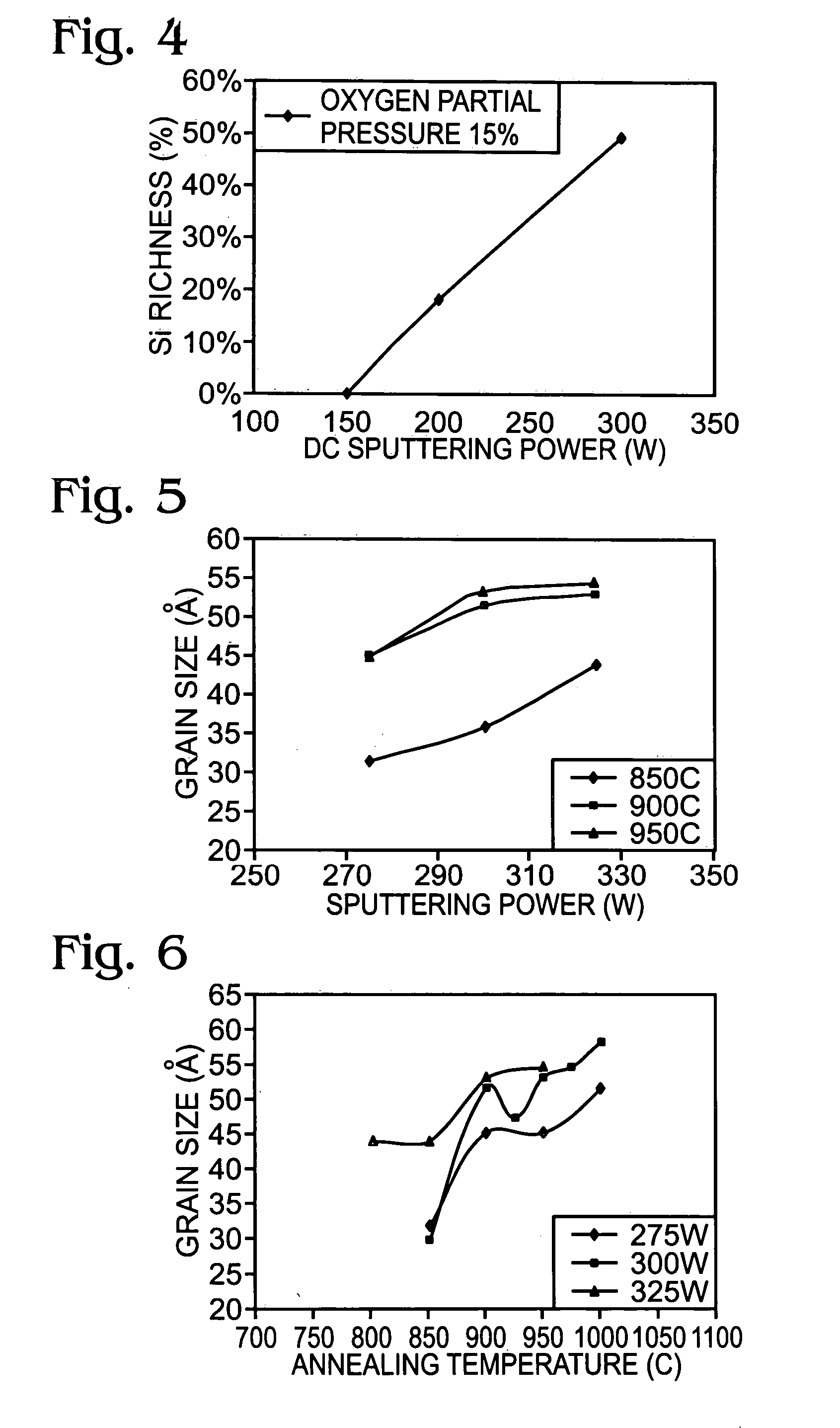
[0027] Defects in the SRSO layer 106 occur as a result of impurities, non-uniformities, vacancies of Si or O, or porosity, to name a few possibilities. Using processes discussed below, impurities can be reduced and improvements made in uniformity, as compared to a conventional implantation process. For example, after thermal annealing, the vacancies of Si or O can be reduced, and the por...


PUM


Abstract

A method is provided for forming a Si electroluminescence (EL) device for emitting light at short wavelengths. The method comprises: providing a substrate; forming a first insulator layer overlying the substrate; forming a silicon-rich silicon oxide (SRSO) layer overlying the first insulator layer, embedded with nanocrystalline Si having a size in the range of 0.5 to 5 nm; forming a second insulator layer overlying the SRSO layer; and, forming a top electrode. Typically, the SRSO has a Si richness in the range of 5 to 40%. In one aspect, the SRSO layer is formed using a DC sputtering process. In another aspect, the SRSO formation step includes a rapid thermal annealing (RTA) process subsequent to depositing the SRSO. Likewise, thermal oxidation or plasma oxidation can be performed subsequent to the SRSO layer deposition. The size of Si nanocrystals is decreased in response to above-mentioned deposition, annealing, and oxidation processes.

Description

BACKGROUND OF THE INVENTION [0001] 1. Field of the Invention [0002] This invention generally relates to integrated circuit (IC) fabrication and, more particularly, to a silicon-based electroluminescence (EL) device that emits light in a wide band of wavelengths. [0003] 2. Description of the Related Art [0004] The generation of light from semiconductor devices is possible, regardless of whether the semiconductor material forms a direct or indirect bandgap. High field reverse biased p-n junctions create large hot carrier populations that recombine with the release of photons. For silicon devices, the light generation efficiency is known to be poor and the photon energy is predominantly around 2 eV. The conversion of electrical energy to optical photonic energy is called electroluminescence (EL). Efficient EL devices have been made that can operate with small electrical signals, at room temperature. However, these devices are fabricated on materials that are typically not compatible wi...

Claims


Application Information

Patent Timeline
IPC IPC(8): H01L29/26
CPCH05B33/145
Inventor LI, TINGKAIGAO, WEIONO, YOSHIHSU, SHENG TENG
Owner SHARP LAB OF AMERICA INC
Why Eureka
Try Eureka