Crystallized semiconductor device, method for producing same and crystallization apparatus

a crystallization apparatus and crystallization technology, applied in the direction of chemistry apparatus and processes, single crystal growth, transistors, etc., can solve the problems of increasing device costs, affecting the price reduction of display devices, and expensive glass substrates capable of meeting high temperature needs, so as to reduce the speed of temperature decrease, reduce the size of the crystal formed in the semiconductor layer, and restrain the effect of the temperature drop

Inactive Publication Date:
View PDF16 Cites 9 Cited by
  • Summary
  • Abstract
  • Description
  • Claims
  • Application Information

AI Technical Summary

Benefits of technology

[0025] Because the crystallization means irradiates the semiconductor layer with the laser light from above the thermal diffusion layer, it is possible to slow down the speed of decrease in temperature of the semiconductor layer molten by the laser light, as compared to the conventional arrangement. Specifically, a part of the laser light having passed through the thermal diffusion layer is accumulated as the heat in the thermal diffusion layer. Then, the accumulated heat is given to the semiconductor layer, so that it becomes possible to restrain a decrease in temperature of the semiconductor layer. In this way, the size of the crystal formed in the semiconductor layer can be increased as compared to the conventional arrangement.
[0026] Moreover, it is possible to provide the crystallization apparatus which can (i) reduce an absorption of the laser light in the thermal diffusion layer and (ii) absorb the laser light greatly in the semiconductor layer, by irradiating the semiconductor layer from above the thermal diffusion layer with the laser light having a wavelength of 550 nm or less. As a result, it becomes possible to increase the efficiency of crystallization of the crystallized semiconductor device, and also possible to reduce manufacturing costs by reducing of a manufacturing time.

Problems solved by technology

Therefore, it becomes unnecessary to separately mount a driver IC and a drive circuit substrate on the display device.
However, in the case of manufacturing the polycrystalline silicone by using the above method, an expensive glass substrate capable of withstanding the high temperature needs to be used as a substrate on which the amorphous silicon is stacked.
This hinders price reduction of the display device.
This causes an increase in device costs.
In addition, because each feeding amount is small, a processing speed is slow.

Method used


Image

  • Crystallized semiconductor device, method for producing same and crystallization apparatus
  • Crystallized semiconductor device, method for producing same and crystallization apparatus
  • Crystallized semiconductor device, method for producing same and crystallization apparatus

Examples


first embodiment

The First Embodiment

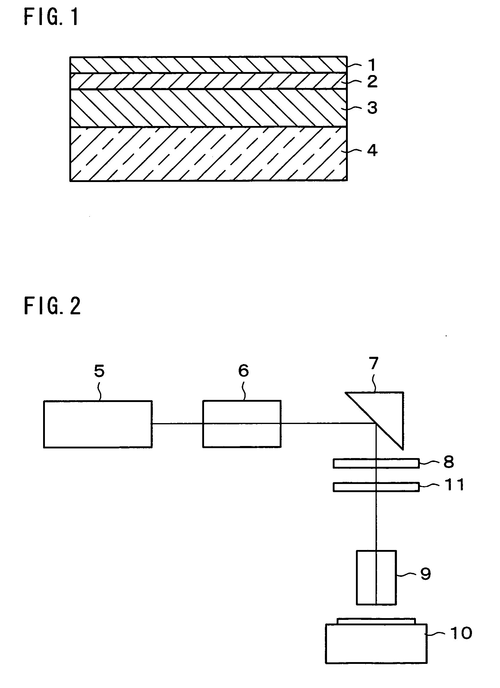
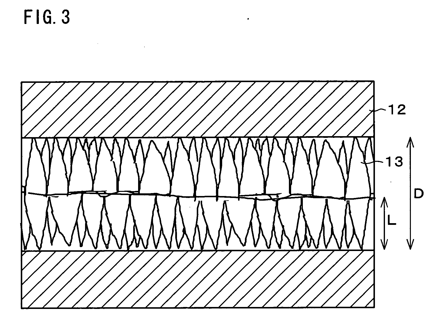
[0036] The following explains one embodiment of the present invention in reference to FIGS. 1 to 8.

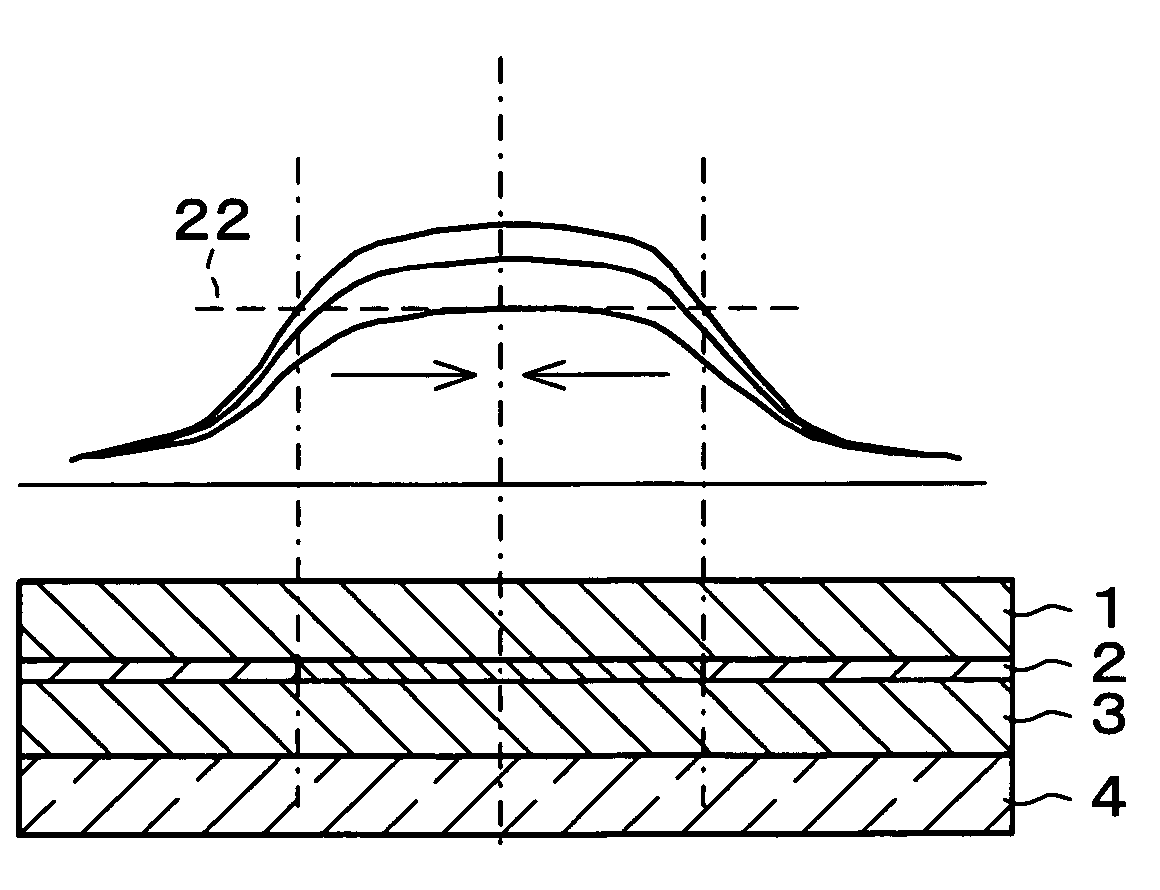
[0037] A method of manufacturing a crystallized semiconductor device in accordance with the present embodiment includes the steps of (i) forming a semiconductor layer on a substrate and (ii) irradiating the semiconductor layer with laser light to crystallize the semiconductor layer. The method further includes the step of forming a thermal diffusion layer on a surface of the semiconductor layer, the thermal diffusion layer having higher thermal conductivity than that of the substrate, and in the step of crystallization (step (ii)), the irradiation of the laser light is carried out from above the thermal diffusion layer.

[0038] A non-crystallized semiconductor device in which the semiconductor layer is not crystallized is so arranged that a thermal diffusion layer having higher thermal conductivity than that of the substrate is formed on a surface of the semiconduct...


PUM

PropertyMeasurementUnit
wavelengthaaaaaaaaaa
optical transmittanceaaaaaaaaaa

Abstract

In a method of manufacturing a crystallized semiconductor device of the present invention, a thermal diffusion layer (1) having higher thermal conductivity than that of a substrate (4) is formed on a surface of a semiconductor layer (2), and then laser light is applied to the semiconductor layer (2) from above the thermal diffusion layer (1). As a result, it becomes possible to manufacture the crystallized semiconductor device in which a crystal is longer than that of a conventional arrangement. According to the present invention, it is possible to provide the crystallized semiconductor device having the semiconductor layer in which the size of the crystal grain is larger than that of the conventional arrangement.

Description

TECHNICAL FIELD [0001] The present invention relates to a method of manufacturing a crystallized semiconductor device manufactured by utilizing laser light, and a crystallization apparatus for crystallizing a semiconductor layer. BACKGROUND ART [0002] A thin film transistor, used in a display device to which liquid crystal, electro luminescence (EL), or the like is applied, uses an active layer made of amorphous silicon or polycrystalline silicon. Because the thin film transistor (crystallized semiconductor device) using the active layer made of the polycrystalline silicon has greater mobility of electron than that of the thin film transistor using the active layer made of the amorphous silicon, the former thin film transistor has many advantages as compared with the latter thin film transistor. [0003] Specifically, for example, in the thin film transistor using the active layer made of the polycrystalline silicon, it is possible to form not only a switching element in a pixel porti...

Claims


Application Information

Patent Timeline
Patent Type & Authority Applications(United States)
IPC IPC(8): H01L21/84C30B11/00H01L21/20H01L21/268H01L21/336H01L29/786
CPCY10T117/1024H01L21/2026H01L21/02686H01L21/02422H01L21/02488H01L21/02532H01L21/02595H01L21/0268H01L21/02675
Inventor INUI, TETSUYATSUNAZAWA, HIROSHIOKAZAKI, SHINYA
Why Eureka
Try Eureka