Bipolar transistor
a transistor and bipolar technology, applied in the field of bipolar transistors, can solve the problems of increasing the depth increasing the variability of the emitter diffusion, and achieve the effect of reducing the parasitic resistance and strong bonding energy
- Summary
- Abstract
- Description
- Claims
- Application Information
AI Technical Summary
Benefits of technology
Problems solved by technology
Method used
Image

Examples
embodiment 1
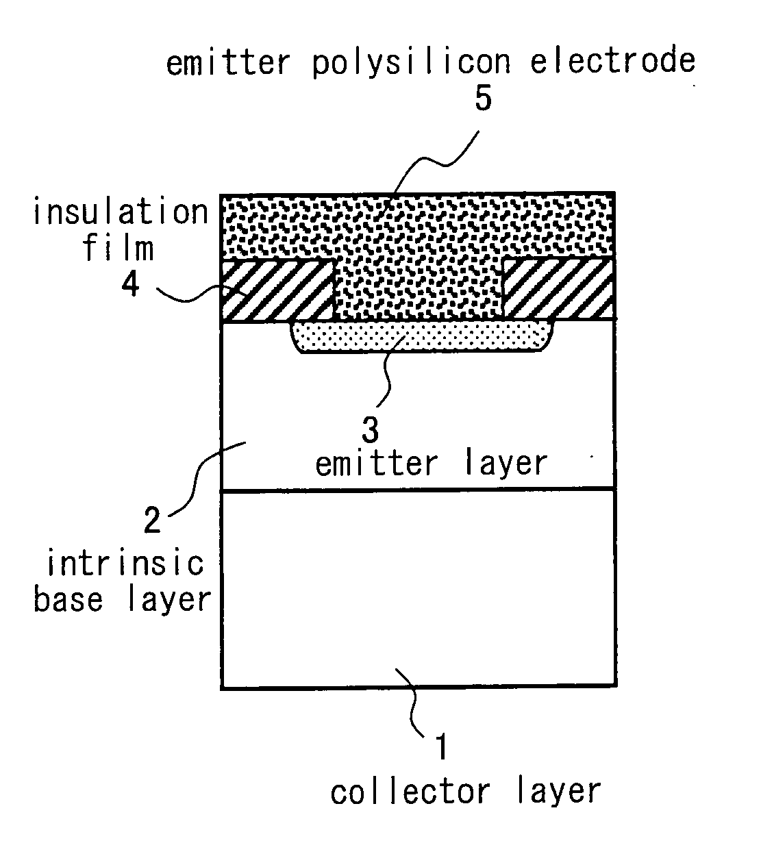
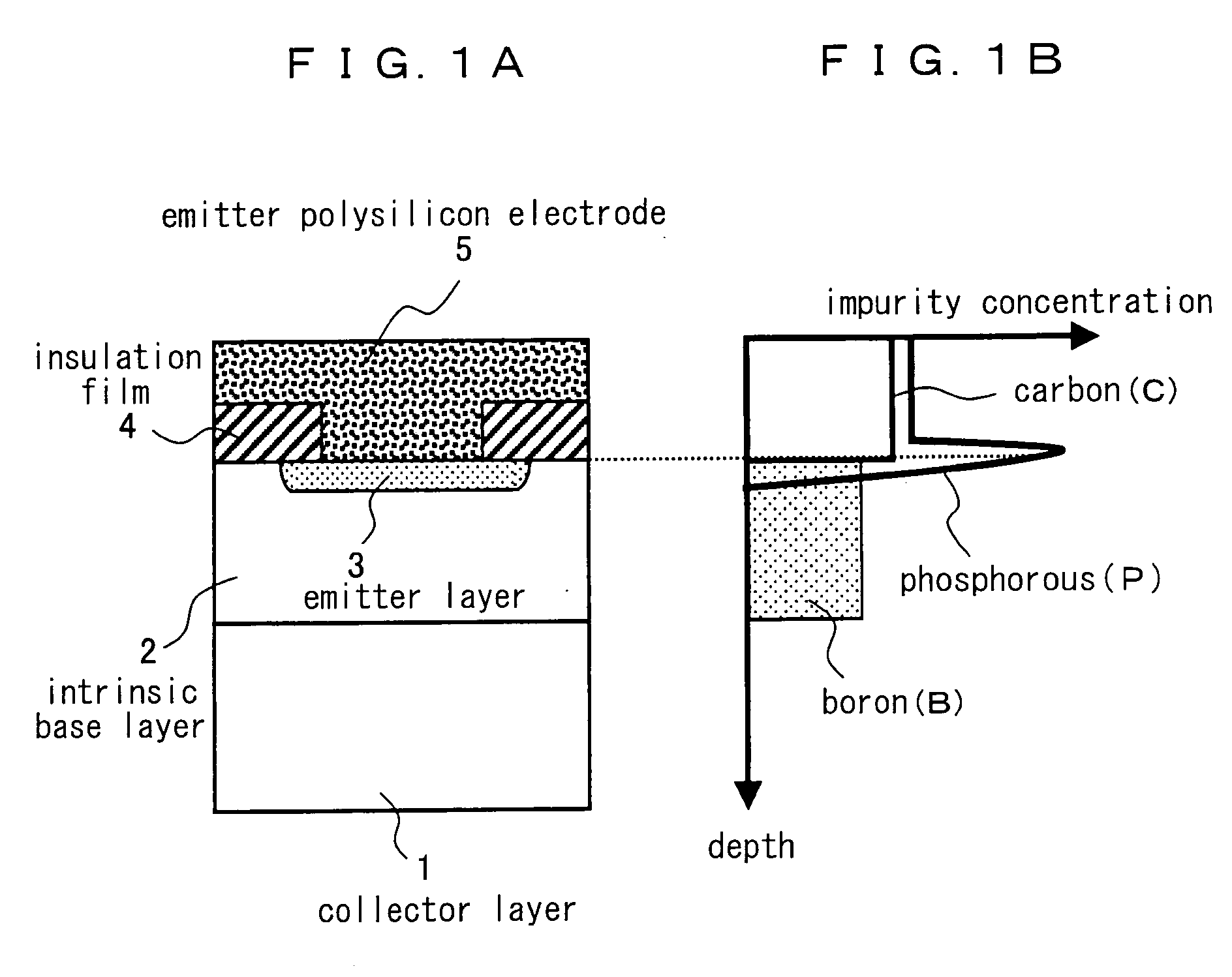
[0054]FIG. 1A is a sectional view illustrating a structure of an emitter section in a bipolar transistor according to an embodiment 1 of the present invention. FIG. 1B shows an impurity concentration profile. In FIGS. 1A and 1B, a reference numeral 1 denotes a collector layer formed in a Si substrate, a reference numeral 2 denotes an intrinsic base layer doped with a P-type impurity such as boron (B) by means of epitaxial growth method on the collector layer 1, a reference numeral 3 denotes an emitter layer formed in the intrinsic base layer 2, a reference numeral 4 denotes an insulation film, and a reference numeral 5 denotes an emitter poly-silicon electrode. The emitter layer 3 is fabricated in such a manner that the emitter poly-silicon electrode 5 is formed and heat treatment is carried out so that an impurity is diffused from the emitter poly-silicon electrode 5 into the intrinsic base layer 2. Referring to any other component in the drawings, the conventional structure shown ...
embodiment 2
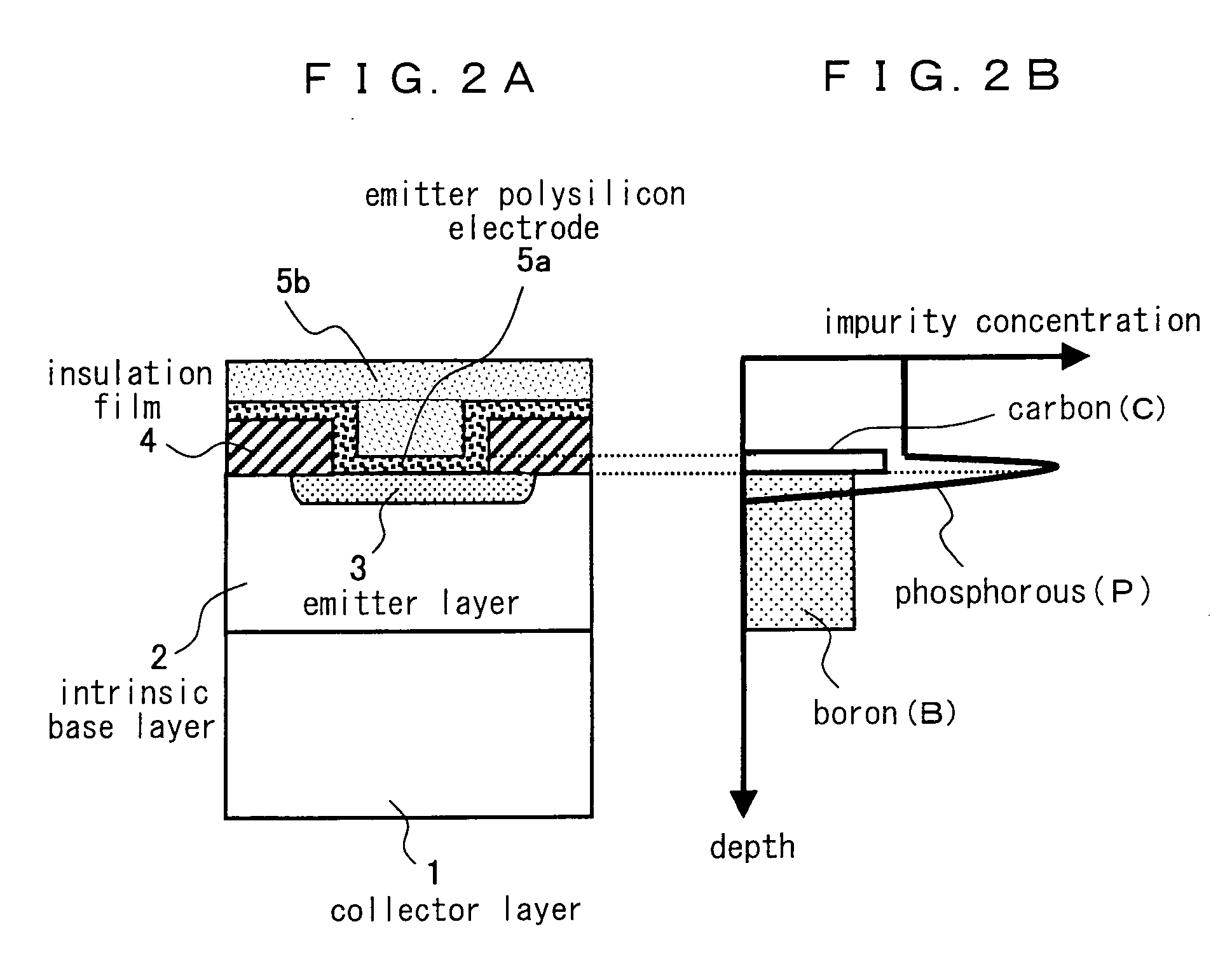
[0062] In an embodiment 2 of the present invention, Ge (germanium) atom as well as C atom are added to the poly-silicon electrode 5 as the outgoing electrode. Namely, the poly-silicon electrode 5 has the composition of Si(1-x-y)GexCy(0<x<1,0<y <<1). An emitter resistance Re can be reduced much more by addition of Ge atom and C atom at the same time. As another advantage, C atom can be added under easier conditions of the film-forming process than in the embodiment 1.
[0063] It is generally known that a Ge semiconductor has a mobility larger than that of the Si semiconductor. Further, it is also well known that the mobility is increased as the cntent of the Ge is increased in a semiconductor made of crystal mixture of Si and Ge. Such a phenomenon can be seen in the same manner in crystal grains in the polycrystalline film. With respect to a conventional poly-silicon electrode, a film resistivity become smaller in the case of a poly-silicon germanium electrode containing germanium in ...
embodiment 3
[0070] It is generally known that the addition of C atom to the poly-silicon increases the resistivity of the film. Then, the resistance Re2 of the poly-silicon electrode 5 increases as the addition amount of C atom become more and more, which, in some case, does not achieve the sufficient effect of the emitter resistance reduction due to the addition of C atom.
[0071] A silicide film 18 is formed on an emitter poly-silicon electrode 17 in order to reduce a contact resistance Re1 between a contact hole 19 and the emitter poly-silicon electrode 17 as shown in the conventional technology in FIG. 4. However, when C atom is added in the such structure mentioned above, a silicide reaction is inhibited, and thereby the disadvantages is caused such as a reduction of thickness and a quality degradation of the silicide film 18.
[0072] An embodiment 3 of the present invention solves the foregoing disadvantages that may be possible to be generated in the embodiments 1 and 2 and thereby further...
PUM
| Property | Measurement | Unit |
|---|---|---|
| thickness | aaaaa | aaaaa |
| thickness | aaaaa | aaaaa |
| thickness | aaaaa | aaaaa |
Abstract
Description
Claims
Application Information
 - R&D
- Intellectual Property
- Life Sciences
- Materials
- Tech Scout
- Unparalleled Data Quality
- Higher Quality Content
- 60% Fewer Hallucinations
Browse by: Latest US Patents, China's latest patents, Technical Efficacy Thesaurus, Application Domain, Technology Topic, Popular Technical Reports.
© 2025 PatSnap. All rights reserved.Legal|Privacy policy|Modern Slavery Act Transparency Statement|Sitemap|About US| Contact US: help@patsnap.com