Donor film and methods for fabricating patterned organic electroluminescent devices using the same

a technology of organic electroluminescent devices and donor films, which is applied in the manufacture of electric discharge tubes/lamps, discharge tubes luminescnet screens, instruments, etc., can solve the problems of large amount of energy required, difficult to achieve micro-patterning, and substantial inability to put into practice, so as to improve the transfer efficiency and facilitate and efficiently manufacture

Inactive Publication Date: 2006-08-24
SAMSUNG DISPLAY CO LTD
View PDF3 Cites 38 Cited by
  • Summary
  • Abstract
  • Description
  • Claims
  • Application Information

AI Technical Summary

Benefits of technology

[0032] According to the present invention, the method of fabricating the organic EL device allows for simultaneous transfer of a metal layer and an organic layer and improved transfer efficiency with a small amount of energy and prevents the organic layer from photo chemical reaction, thus enabling patterned organic EL devices to be easily and efficiently manufactured by a single process.

Problems solved by technology

According to this approach, since the organic layer is liable to deform due to an organic solvent used during the process or developer residues, it is substantially impossible to put into practice.
Another approach is a vacuum deposition method using a mask, which is, however, disadvantageous in that micro-patterning is difficult to achieve.
However, in the case where a pattern is transferred using the laser induced thermal imaging (LITI) method, since a donor film has poor flexibility and poor adhesion between the donor film and a lower acceptor film, a large amount of energy is required.
In addition, since only organic materials are transferable, it is necessary to separately deposit a metal after patterning an organic layer to fabricate a passive matrix type organic EL device, which is quite burdensome.
In this case, however, since a large amount of pressure and a metal-metal adhesive force are used, this method is restrictively applied to metals having a high work function, or alloys of these metals, such as Au—Au, Ag—Ag, Pd—Pd.
In addition, since this method is a lift-off method, rather than a transfer method, it is used only for patterning purposes after fabrication of a device.
In this case, however, since sufficiently large amount of pressure is used and glass mold is used, the organic layer may be physically damaged and a release promotion layer is essentially needed.

Method used


Image

  • Donor film and methods for fabricating patterned organic electroluminescent devices using the same
  • Donor film and methods for fabricating patterned organic electroluminescent devices using the same
  • Donor film and methods for fabricating patterned organic electroluminescent devices using the same

Examples


example 1

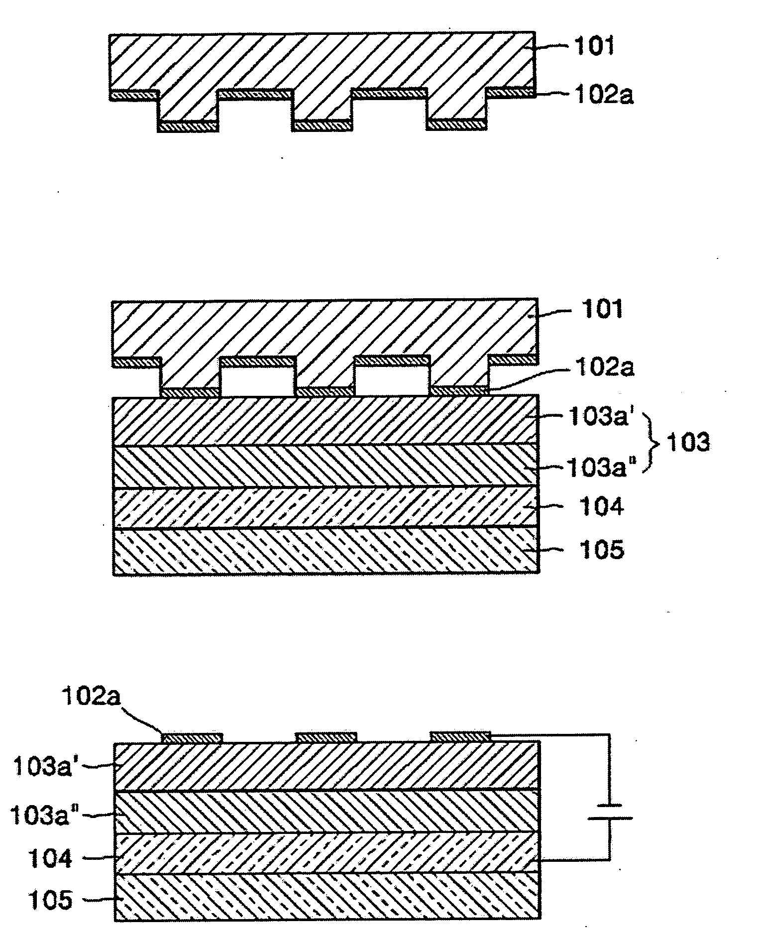
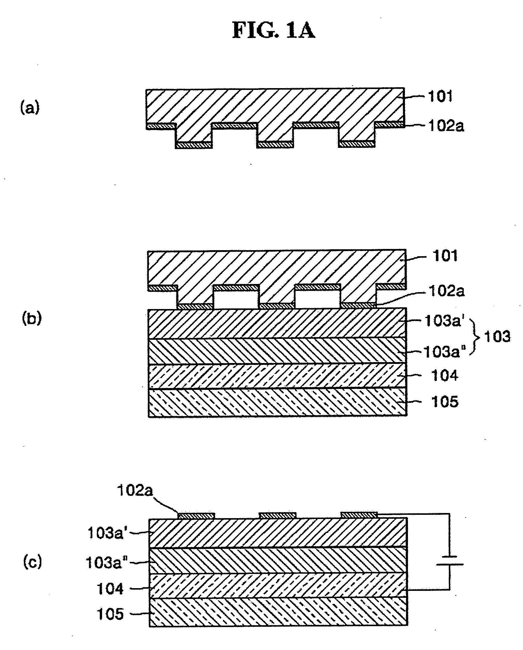
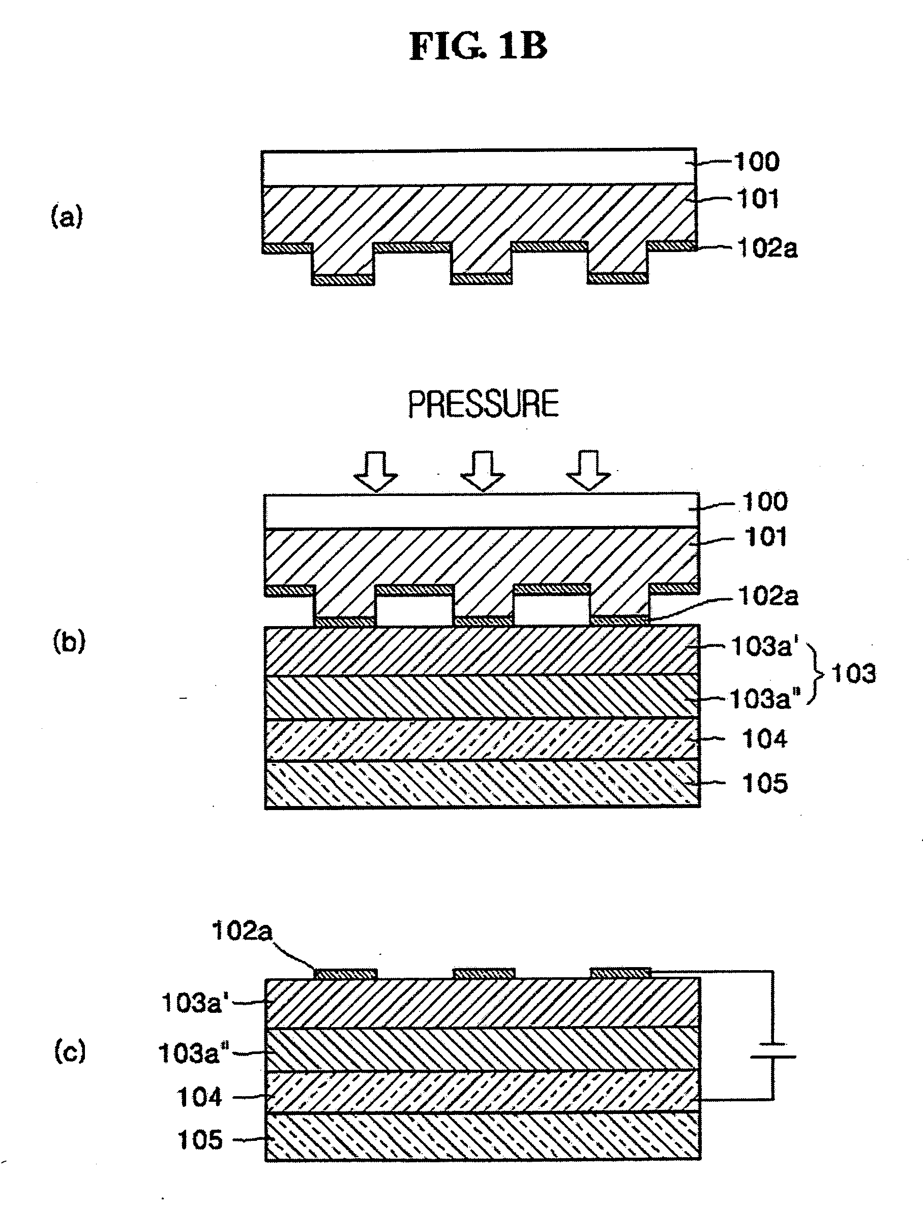
[0078] Preparation of Donor Film for Thin Film Layer (Transfer Layer: Metal Layer Only)

[0079] Sylgard 184A and Sylgard 184B (manufactured from Dow Corning Inc.) were mixed in a stirring vessel in a weight ratio of 10:1 to give a PDMS forming solution. The resulting PDMS forming solution was poured into a master formed of a separately prepared wafer. The master has a striped pattern. Bubbles in the PDMS forming solution poured into the master were removed using a vacuum pump, followed by curing the PDMS forming solution in an oven at a temperature ranging from about 60° C. to about 80° C. and removing the master from the resultant structure, thereby obtaining a PDMS film layer.

[0080] Au was deposited on a patterned surface of the obtained PDMS film layer to a thickness of 20 nm by electron beam deposition under vacuum of 1×10⁻⁷ torr.

[0081] Fabrication of Patterned Organic EL Device

[0082] A glass substrate and 15 Ω / cm2 (1200 Å) ITO as a first electrode cut into a size of 50 mm×50 ...

example 2

[0083] Preparation of Donor Film for Thin Film Transfer (Transfer Layer: Organic Layer Only)

[0084] Sylgard 184A and Sylgard 184B (manufactured from Dow Corning Inc.) were mixed in a stirring vessel in a weight ratio of 10:1 to give a PDMS forming solution. The resulting PDMS forming solution was poured into a master formed of a separately prepared wafer. The master has a striped pattern. Bubbles in the PDMS forming solution poured into the master were removed using a vacuum pump, followed by curing the PDMS forming solution in an oven at a temperature ranging from about 60° C. to about 80° C. and removing the master from the resultant structure, thereby obtaining a PDMS film layer.

[0085] Alumina quinine (Alq3) was deposited on a patterned surface of the obtained PDMS film layer to a thickness of 30 nm under vacuum of 1×10⁻⁷ torr to be used as a second organic layer forming an electron transport layer.

[0086] Fabrication of Patterned Organic EL Device

[0087] A glass substrate and 1...

example 3

[0088] Preparation of Donor Film for LITI (Transfer Layer: Metal Layer and Organic Layer)

[0089] Sylgard 184A and Sylgard 184B (manufactured from Dow Corning Inc.) were mixed in a stirring vessel in a weight ratio of 10:1 to give a PDMS forming solution. The resulting PDMS forming solution was poured into a master formed of a separately prepared wafer. The master has a striped pattern. Bubbles in the PDMS forming solution poured into the master were removed using a vacuum pump, followed by curing the PDMS forming solution in an oven at a temperature ranging from about 60° C. to about 80° C. and removing the master from the resultant structure, thereby obtaining a PDMS film layer.

[0090] Au was deposited on a patterned surface of the obtained PDMS film layer to a thickness of 20 nm by electron beam deposition, Ca was deposited thereon to a thickness of 5 nm by thermal deposition, and a second organic layer made of alumina quinine (Alq3) as a potential electron transport layer was dep...


PUM

PropertyMeasurementUnit
thicknessaaaaaaaaaa
work functionaaaaaaaaaa
temperatureaaaaaaaaaa

Abstract

A donor film has a soft polymer film and a transfer layer to be transferred which is formed on the soft polymer film. When fabricating a patterned organic electroluminescent device using the donor film for thin film transfer, the transfer layer is transferred even with a small amount of energy due to good adhesion between the transfer layer of the donor film and an acceptor film, and multiple layers, such as organic small molecular and polymer layers in addition to a metal layer, may be simultaneously transferred, while eliminating a need of a photothermal conversion layer.

Description

CROSS-REFERENCE TO RELATED PATENT APPLICATION AND CLAIM OF PRIORITY [0001] This application claims the benefit of Korean Patent Application No. 10-2005-0010616, filed on Feb. 4, 2005, in the Korean Intellectual Property Office, the disclosure of which is incorporated herein in its entirety by reference. BACKGROUND OF THE INVENTION [0002] 1. Field of the Invention [0003] The present invention relates to a donor film and methods for fabricating patterned organic electroluminescent devices using the donor film, and more particularly to methods for fabricating patterned organic electroluminescent devices using a donor film for thin film transfer, in which at least one of an organic layer and a metal layer are transferred from an upper donor layer to a lower acceptor layer by at least one of light, heat, electric energy and pressure, the donor film containing a soft polymer film layer having a glass transition temperature of not greater room temperature. [0004] 2. Description of the Rela...

Claims


Application Information

Patent Timeline
Patent Type & Authority Applications(United States)
IPC IPC(8): B32B3/00H01L51/56H01L51/50
CPCH01L51/0013Y10T428/2457Y10T428/24479H10K71/18H05B33/10
Inventor LEE, TAE-WOO
Owner SAMSUNG DISPLAY CO LTD
Why Eureka
Try Eureka