Method for measurement of gas flow velocity, method for energy conversion using gas flow over solid material, and device therefor
a gas flow velocity and gas flow technology, applied in the direction of liquid/fluent solid measurement, generator/motor, instruments, etc., can solve the problems of limited application of this method, dependant method, large equipment required (lasers, ccd cameras) and large size of equipment, etc., to achieve low response time, small construction size, and low cost
- Summary
- Abstract
- Description
- Claims
- Application Information
AI Technical Summary
Benefits of technology
Problems solved by technology
Method used
Image
Examples
example 1
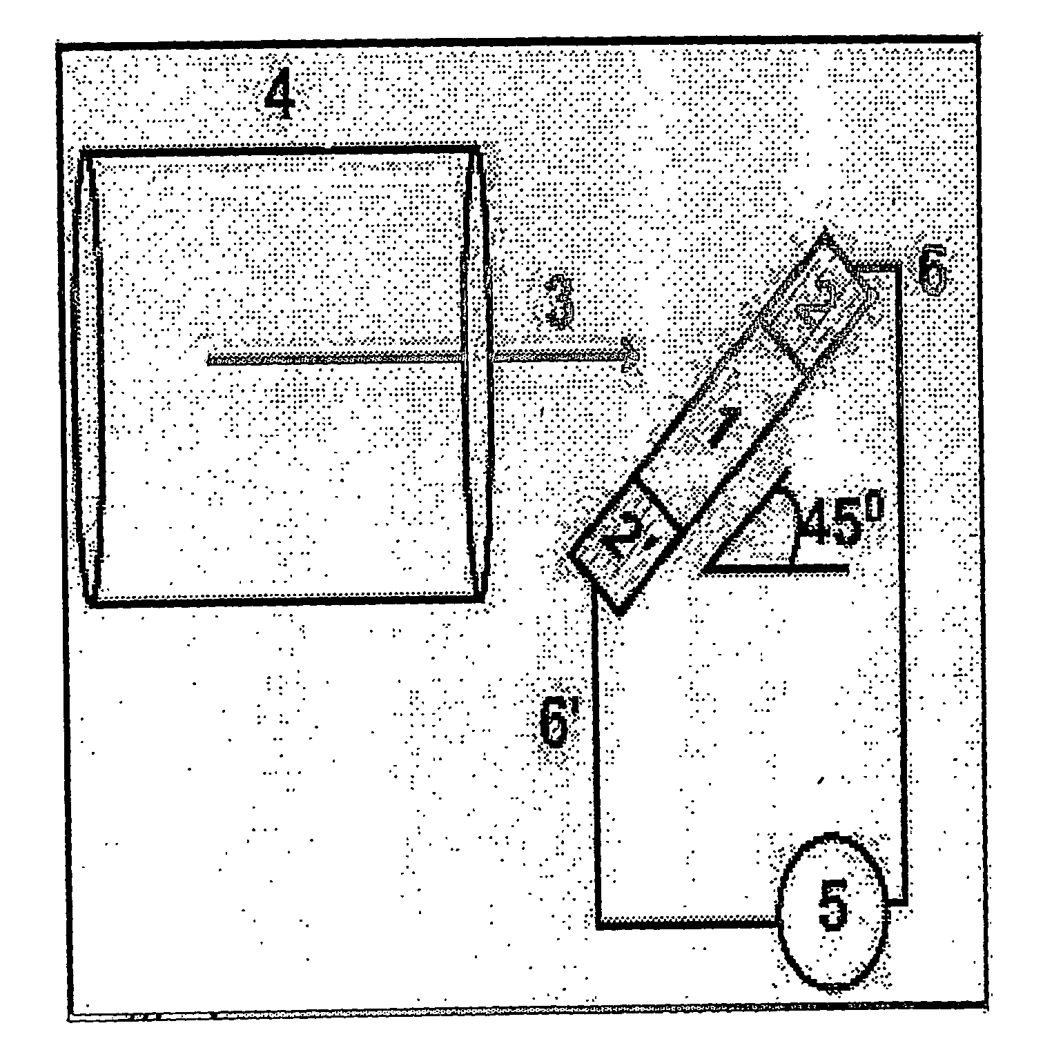
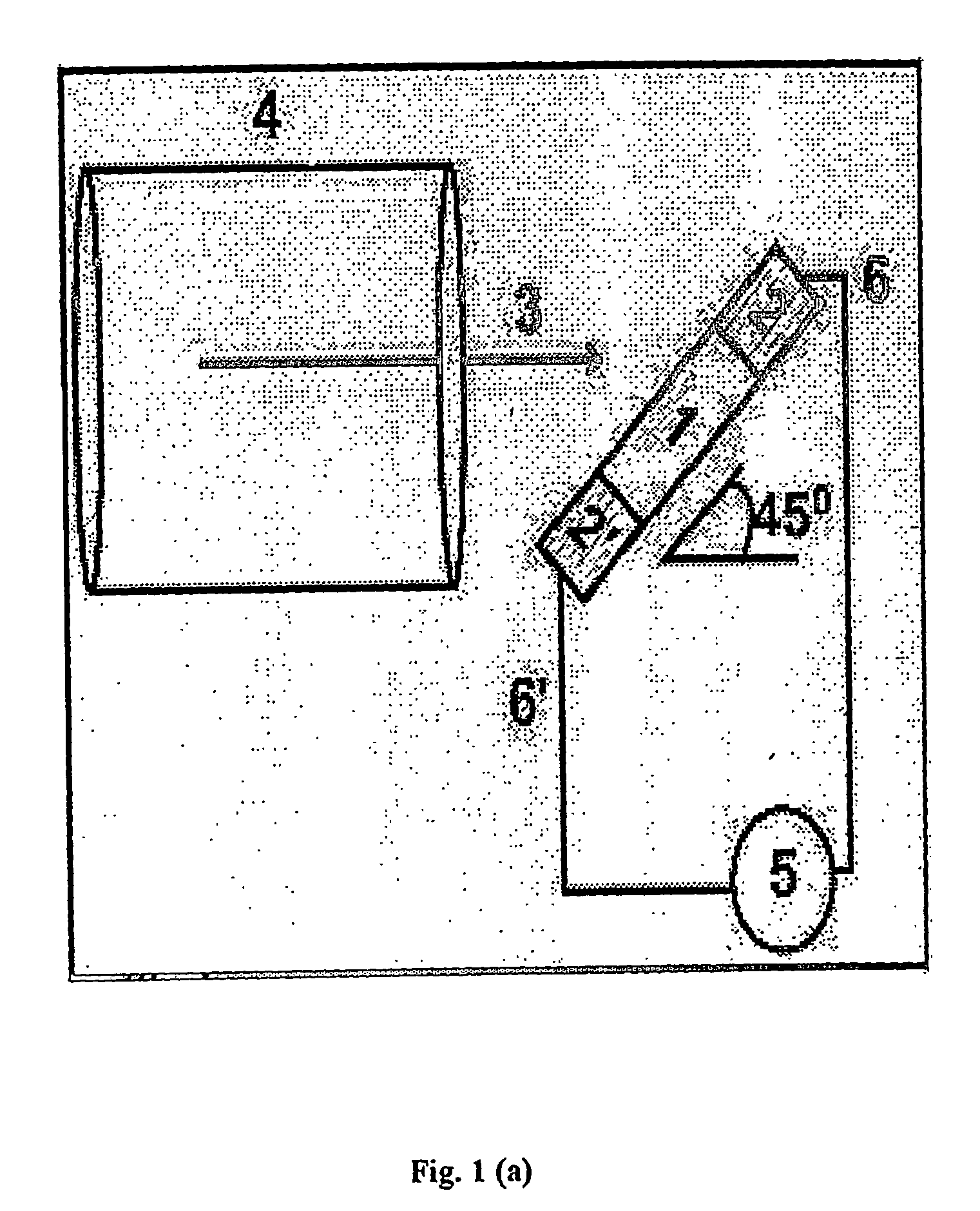
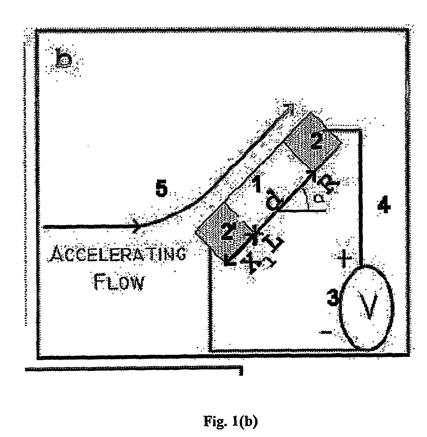
[0133]FIG. 1(d) shows a schematic layout of the experimental set up used in example 1 to achieve a calibrated gas flow velocity in the flow sensing device of the invention. Flow sensing devices comprising 3×10⁻³ m along the gas flow and 1×10⁻³ m perpendicular to the gas flow were used. The flow sensing elements were made of n-type Ge (Sb doped, ρ=0.01 Ωm), n-Si (ρ=0.01 Ωcm), p-Si (ρ=0.01 Ωcm), single wall carbon nanotubes, multi-wall carbon nanotubes, graphite and polycrystalline copper. The electrical contacts comprised of copper leads of 125×10−6 m diameter made using silver emulsion (shown in the shaded region in FIG. 1(b)). The exposed area of the flow sensor element is not covered by the silver emulsion and was about 2×10⁻³ m along the flow and 1×10⁻³ m perpendicular to the flow of the gas. The sensing elements comprising single wall carbon nanotubes, multi-wall carbon nanotubes, and graphite were prepared by densely packing the powder between the two electrodes. The dimensions...
example 2
[0136] The same set up as in Example 1 was repeated except that the flow sensor element was kept at a distance of 2×10⁻² m from the exit point or 1×10⁻² m outside the tube. The results obtained were similar to those in Example 1.
example 3
[0137] The same experiment was repeated as in Example 1 except that the material in question was a solid polycrystalline copper sheet for which the slope of A was very small. The results are given in Table 1.
[0138] A comparison of the various results obtained show that the signal for p-type Si and SWNT are opposite to that for n-type Si, n-Ge, graphite and copper. SWNT samples are usually unintentionally p-doped (Hone et al, Phys. Rev. Lett., 80, 1042, 1998 [4]; and Collins et al, Science, 287, 1801, 2000) [3]. This explains the sign of the flow induced voltage being the same for SWNT and p-Si. The inset of FIG. 3 shows the plot of the slope A versus the Seebeck coefficients (S) of the solid materials used. The coefficient A depends linearly on S as shown by the fitted line in the inset with slope=60K.
PUM
 Abstract
Description
Claims
Application Information


