Plasma processing apparatus and semiconductor device manufactured by the same apparatus

a technology of processing apparatus and semiconductor device, which is applied in the direction of coating, chemical vapor deposition coating, electric discharge tube, etc., can solve the problems of high cost, serious cost, and natural cos

Inactive Publication Date: 2006-08-31
SHARP KK
View PDF34 Cites 18 Cited by
  • Summary
  • Abstract
  • Description
  • Claims
  • Application Information

AI Technical Summary

Benefits of technology

[0020] The present invention has been devised in view of such circumstances, and it is an object of the present invention to provide a plasma processing apparatus which can evenly introduce reactive material gas into a plurality of discharge spaces in the plasma processing apparatus in which a plurality of sets of cathode-anode bodies for performing plasma discharge by reactive material gas are provided inside the chamber, and a semiconductor device manufactured by this plasma processing apparatus.

Problems solved by technology

Furthermore, it is also required that a needle valve in each gas introduction pipe 10 after branching is provided for the purpose of improving difference in conductance caused by difference in piping length; therefore, it naturally becomes high cost.
The gas introduction pipe 10 is required to use stainless steel pipe with high airtightness because gas to be introduced to the discharge space is accompanied with high danger when gas such as special high pressure gas or hydrogen leaks and the port is required to provide the number corresponding to those of the discharge spaces, resulting in further high cost.
Furthermore, since the entire distance of the gas introduction system is long compared to the case where simple connection is made with a single pipe and the number of valves is many, delicate consideration is required for safety of exhaust ventilation at the branch section, and consequently it becomes a serious cost.
Further, in the case where gas is introduced to the cathode 2, since insulation needs to be provided between the stainless steel pipe which introduces gas to the individual discharge spaces and the cathode, it is required to connect by sandwiching an expensive insulating insulator, resulting in high cost.
Furthermore, since there is no material having considerably high heat resistance in processable insulating components, in the case where temperature of the cathode 2 becomes approximately 180° C. or more, a water cooling pipe is required for the purpose of cooling this part, and consequently it becomes a serious cost.
However, in the case where gas is simultaneously supplied to a plurality of discharge spaces, when piping lengths for introducing gas are largely different as shown in the drawing, the gas cannot be equally introduced into the respective discharge spaces.
If the gas is evenly introduced into the respective discharge spaces with this configuration, a needle valve needs to be provided in each gas introduction pipe after branching as in the apparatus shown in FIG. 5, and consequently it becomes a serious cost.

Method used


Image

  • Plasma processing apparatus and semiconductor device manufactured by the same apparatus
  • Plasma processing apparatus and semiconductor device manufactured by the same apparatus
  • Plasma processing apparatus and semiconductor device manufactured by the same apparatus

Examples


first embodiment

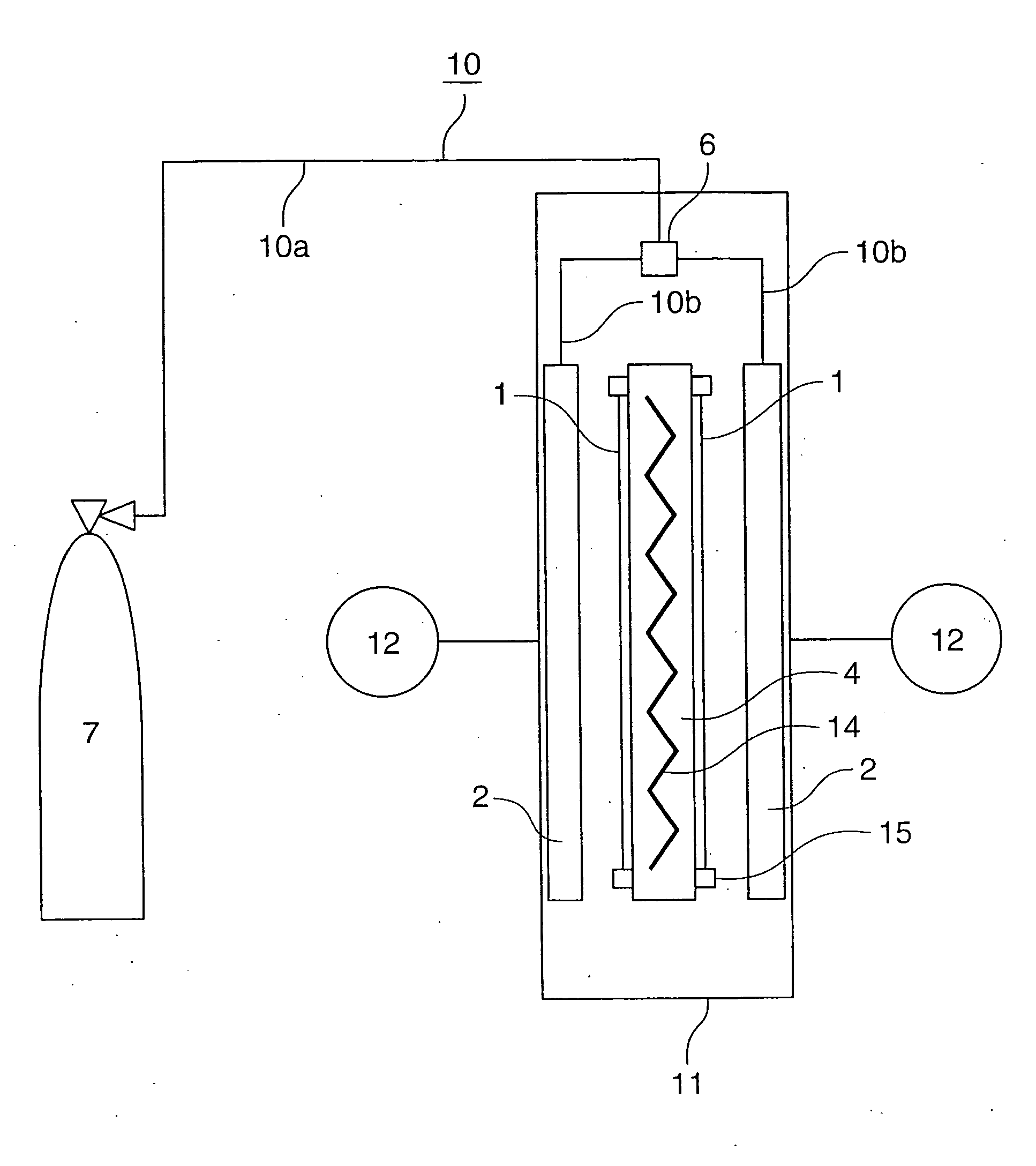
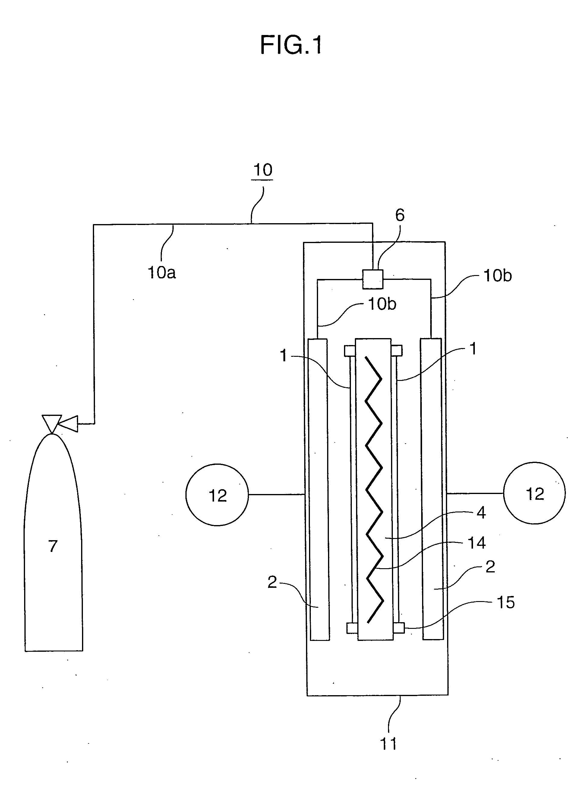
[0044]FIG. 1 is a schematic longitudinal sectional view showing a semiconductor device manufacturing apparatus as a plasma processing apparatus according to a first embodiment.

[0045] In the semiconductor device manufacturing apparatus, an anode 4 and cathodes 2, 2 are arranged so that the anode 4 is sandwiched by the cathodes 2, 2 with a predetermined interval in a horizontal direction. Then, plasma discharge is performed at spaces (two discharge spaces) between the anode 4 and each of the cathodes 2, 2 with reactive material gas introduced into a chamber 11.

[0046] The semiconductor device manufacturing apparatus will be more specifically described. That is, the semiconductor device manufacturing apparatus comprises the chamber 11 which is sealable vertical type as a reactive vessel, and one anode 4 is substantially vertically arranged with respect to a bottom surface of the chamber 11 at its inside center portion. Glass substrates 1, 1, which are materials to be processed, are ar...

second embodiment

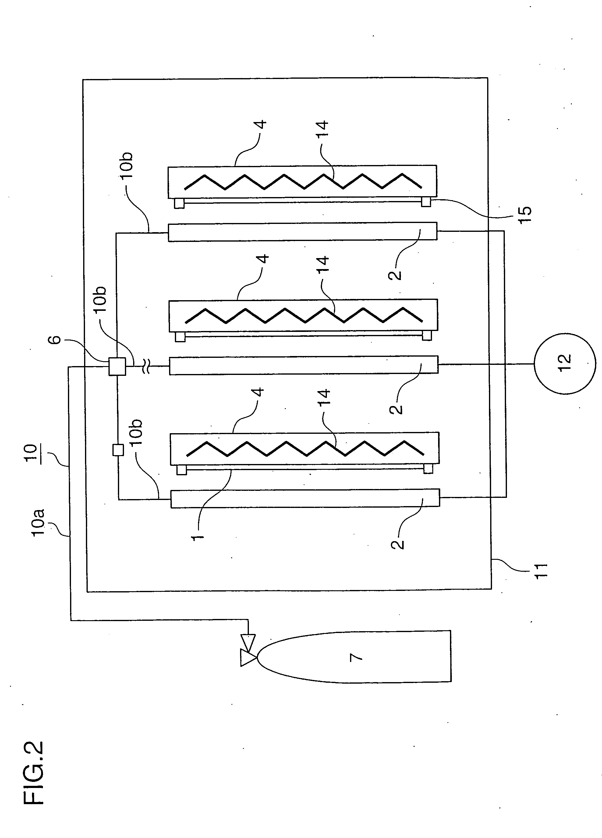
[0062]FIG. 2 is a schematic longitudinal sectional view showing a semiconductor device manufacturing apparatus as a plasma processing apparatus according to a second embodiment.

[0063] In a sealable vertical chamber 11, three sets of cathode-anode bodies are substantially vertically arranged with respect to a bottom surface of the chamber 11. Then, plasma discharge is performed at spaces (three discharge spaces) between the anodes 4 and the cathodes 2 in the cathode-anode bodies with reactive material gas introduced into the chamber 11. The cathode-anode bodies are made up of three sets for simplification in FIG. 2; however, it is not limited to this. The anode 4 in the cathode-anode bodies is made of material having conductivity and heat resistance, such as stainless steel, aluminum alloy, and carbon.

[0064] Although not shown in FIG. 2, similar to FIG. 5, a pressure controller 22 and a vacuum pump 21 are provided in order to flexibly control pressure of reactive gas in the chamber...

third embodiment

[0078]FIG. 3 is a schematic longitudinal sectional view showing a semiconductor device manufacturing apparatus as a plasma processing apparatus according to a third embodiment.

[0079] The semiconductor device manufacturing apparatus of FIG. 3 has the same configuration as the second embodiment, but uses material gas different from that of the second embodiment. That is, this semiconductor device manufacturing apparatus uses gas fluorine-based material gas (here, NF3) diluted with inert gas (here, Ar) for etching apparatus. Electric power is supplied to the cathodes 2, 2, 2 by the plasma excitation power supplies 12 as in the same condition of the first embodiment.

[0080] According to this semiconductor device manufacturing apparatus, etching of silicon film can be performed on the surface of the substrates 1, 1, 1 at a speed of 10 nm / s or more.

[0081] The plasma processing apparatus (semiconductor device manufacturing apparatus) according to the third embodiment is configured as the...


PUM

PropertyMeasurementUnit
constant temperatureaaaaaaaaaa
temperatureaaaaaaaaaa
heat resistance temperatureaaaaaaaaaa

Abstract

A plasma processing apparatus of this invention includes a sealable chamber, a gas supply source of reactive material gas, placed outside the chamber, a gas introduction pipe connected to the gas supply source, for introducing the material gas into the chamber, and a plurality of sets of cathode-anode bodies for forming a plurality of discharge spaces which perform plasma discharge of the material gas in the chamber. Herein, the gas introduction pipe includes a gas branch section arranged in the chamber, a main pipe for connecting the gas supply source to the gas branch section, and a plurality of branch pipes connected from the main pipe to each of the discharge spaces via the gas branch section. The branch pipes are configured so that conductances thereof are substantially equivalent to each other.

Description

CROSS-REFERENCE TO RELATED APPLICATION [0001] This application is related to Japanese Patent Application No. 2005-006598 filed on Jan. 13, 2005, on the basis of which priority is claimed under 35 USC §119, the disclosure of this application being incorporated by reference in its entirety. BACKGROUND OF THE INVENTION [0002] 1. Field of the Invention [0003] The present invention relates to a plasma processing apparatus and a semiconductor device manufactured by the same apparatus. More particularly, the present invention relates to a plasma processing apparatus which is for use in manufacturing a semiconductor device by plasma discharge of reactive material gas in a sealable chamber, for example, by processing a substrate which is a material to be processed, and in which a plurality of sets of cathode-anode bodies for performing plasma discharge are provided in the chamber so that a plurality of discharge spaces exist, and also relates to a semiconductor device manufactured by this pl...

Claims


Application Information

Patent Timeline
Patent Type & Authority Applications(United States)
IPC IPC(8): C23F1/00C23C16/00
CPCH01J37/3244
Inventor KISHIMOTO, KATSUSHIFUKUOKA, YUSUKE
Owner SHARP KK
Why Eureka
Try Eureka