
Method for forming film

a film and film technology, applied in the direction of coatings, chemical vapor deposition coatings, semiconductor devices, etc., can solve the problems of affecting the effect of film forming, and destroying the diffusion layer formed in the silicon layer, etc., to achieve less micro cracks, less peeling off, and effective resolution

Inactive Publication Date: 2006-08-31
TOKYO ELECTRON LTD
View PDF12 Cites 156 Cited by
  • Summary
  • Abstract
  • Description
  • Claims
  • Application Information

AI Technical Summary

Benefits of technology

[0010] This invention is developed by focusing the aforementioned problems in order to resolve them effectively. An object of the present invention is to provide a film-forming method of a metal-nitride film in which less micro cracks and less peeling off may occur even at a relatively high temperature.
[0012] According to the above feature, although the film-forming process is conducted at a relatively high temperature, a metal-nitride film can be deposited whose chlorine density is low, whose resistivity is low, and in which fewer cracks may be generated.

Problems solved by technology

However, when a tungsten film is formed directly onto a silicon layer or an aluminum wiring which is a lower layer, a diffusion layer formed in the silicon layer is destroyed by an attack of fluorine and / or an adhesiveness to an upper layer becomes worse, at a boundary portion therebetween.
The reason of conducting the post-flow step is that if any Cl element remains in the film, resistivity of the film may increase and / or corrosion thereof may occur.
However, the inventor has found that micro cracks may be generated when a film thickness of the deposited TiN film is thickened over a certain degree.

Method used


Image

  • Method for forming film
  • Method for forming film
  • Method for forming film

Examples


first embodiment

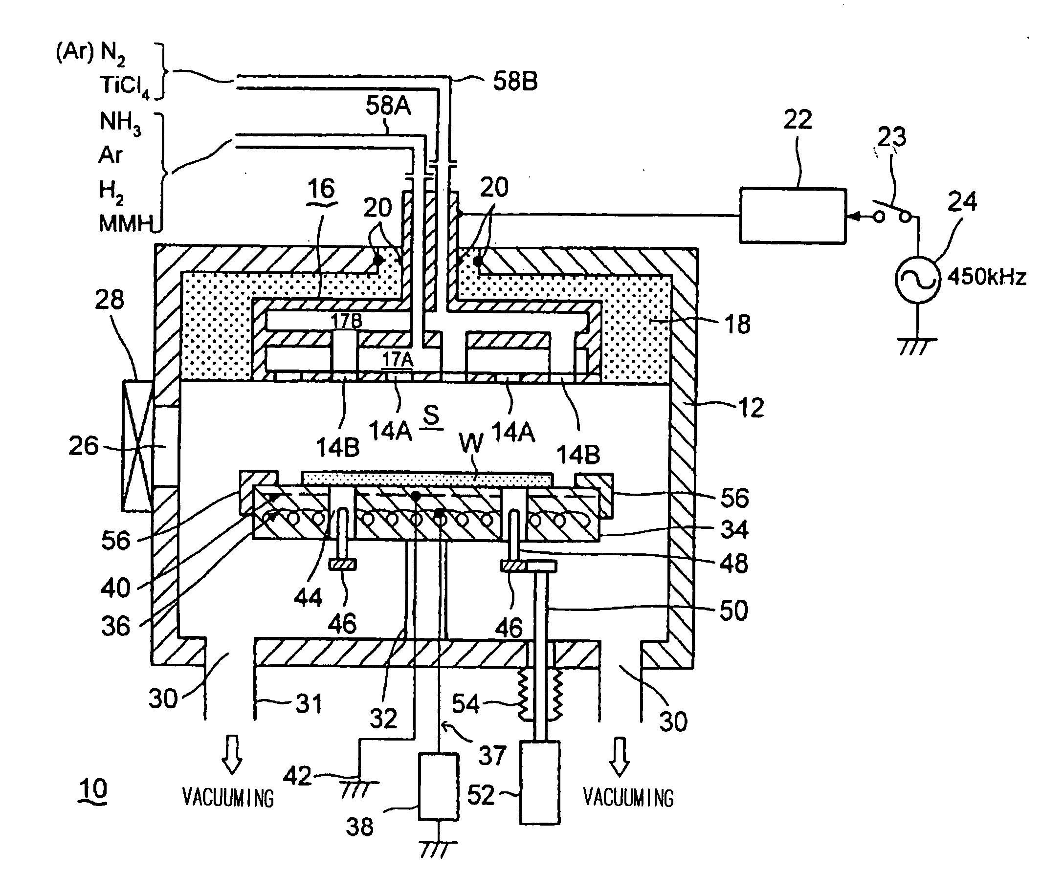
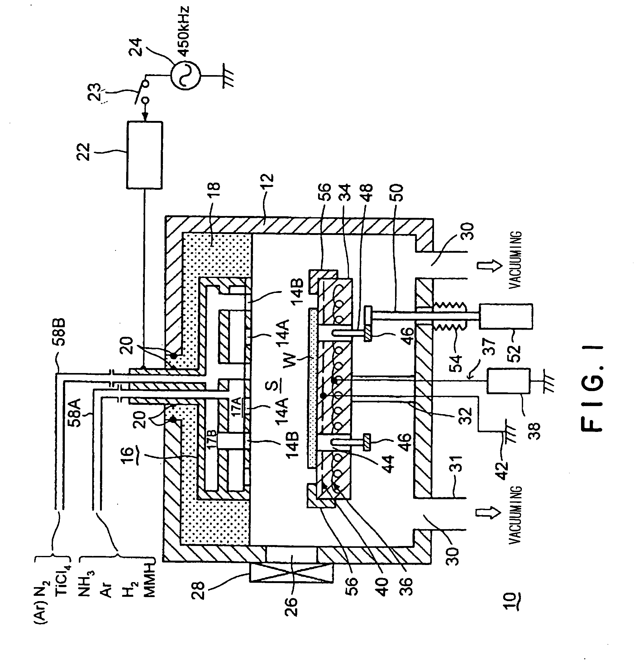
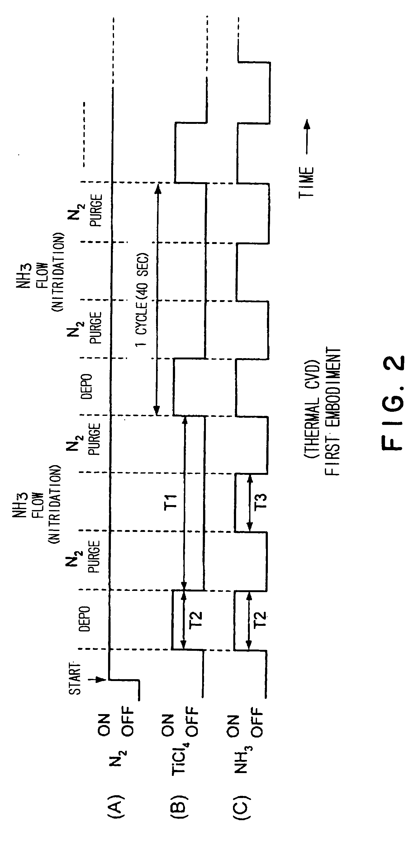
[0058]FIG. 1 is a schematic cross sectional view showing an example of processing unit for carrying out a film-forming method according to the present invention, and FIG. 2 is a chart showing timings of supply of various gases in a first embodiment according to the present invention. Herein, a case is explained as an example, wherein the processing unit is a plasma CVD film-forming unit and the metal-nitride film is a TiN film. The plasma CVD film-forming unit may be also used as a thermal CVD film-forming unit if a high-frequency voltage is not applied thereto so that no plasma is generated.

[0059] As shown in FIG. 1, the plasma CVD film-forming unit 10 as a processing unit has a processing container 12 formed cylindrically and made of, for example, nickel or a nickel alloy. A ceiling part of the processing container 12 is provided with a showerhead 16, which has a large number of gas-jetting holes (ways) 14A, 14B in a lower surface thereof. Thus, a process gas such as a film-formin...

second embodiment

[0102] Next, the present invention is explained.

[0103]FIG. 9 is a chart showing timings of supply of various gases in the second embodiment according to the present invention.

[0104] Herein, an inert gas and a nitrogen-including reduction gas are continuously supplied, while a metal source gas is intermittently supplied. That is, an N2 gas as the inert gas and an NH3 gas as the nitrogen-including reduction gas are continuously supplied, while a TiCl4 gas as the metal source gas is intermittently supplied in accordance with a pulse-pattern in time. Thus, a TiN film is deposited by a thermal CVD. Then, a step cycle of DEPO→NH3 FLOW (nitridation) (→DEPO→NH3 FLOW (nitridation)) . . . is repeated in sequence. In the case shown in FIG. 9, a supply term T2 and a non-supply term T1 of the TiCl4 gas are set to substantially the same term. In addition, the term of the cycle is for example about 30 seconds.

[0105] In the second embodiment as well, it is possible to lower chlorine density that ...

third embodiment

[0118] Next, the present invention is explained.

[0119]FIG. 12 is a chart showing timings of supply of various gases in the third embodiment according to the present invention.

[0120] Herein, an inert gas is continuously supplied, while a metal source gas is intermittently supplied. A nitrogen-including reduction gas is supplied during the supply terms T2 of the metal source gas, for terms T6 shorter than the supply terms T2, and also during the non-supply terms T1 of the metal source gas, for terms T3 shorter than the non-supply terms T1.

[0121] That is, an N2 gas as the inert gas is continuously supplied, while a TiCl4 gas as the metal source gas is intermittently supplied in accordance with a pulse-pattern in time. In addition, the NH3 gas as the nitrogen-including reduction gas is supplied in accordance with a pulse-pattern in time, that is, for the terms T6 and T3 that are respectively shorter than the supply terms T2 and the non-supply terms T1 of the TiCl4 gas, during the supp...


PUM

PropertyMeasurementUnit
Temperatureaaaaaaaaaa
Thicknessaaaaaaaaaa

Abstract

The present invention relates to a method of forming a metal-nitride film onto a surface of an object to be processed in a processing container in which a vacuum can be created. The method of the invention includes: a step of continuously supplying an inert gas into a processing container set at a high film-forming temperature; and a step of intermittently supplying a metal-source gas into the processing container, during the step of continuously supplying the inert gas. During the step of intermittently supplying the metal-source gas, a nitrogen-including reduction gas is supplied into the processing container at the same time that the metal-source gas is supplied, during a supply term of the metal-source gas. The nitrogen-including reduction gas is also supplied into the processing container for a term shorter than a non-supply term of the metal-source gas, during the non-supply term of the metal-source gas. A film thickness of the metal-nitride film formed during the one supply term of the metal-source gas is not more than 60 nm. According to the invention, although the film-forming process is conducted at a relatively high temperature, a metal-nitride film can be deposited whose chlorine density is low, whose resistivity is low, and in which fewer cracks may be generated.

Description

FIELD OF THE INVENTION [0001] The present invention relates to a film-forming method for depositing a metal-nitride film such as a TiN (Titanium nitride) film onto a surface of an object to be processed such as a semiconductor wafer. DESCRIPTION OF THE RELATED ART [0002] In general, a circuitry is often composed by a multilevel interconnection structure in a semiconductor device in response to a request for recent enhanced density and enhanced integration. In this case, a technique for filling a contact hole, which is a connection part between a lower-layer device and an upper-layer aluminum wiring, and a via hole, which is a connection part between a lower-layer aluminum wiring and an upper-layer aluminum wiring, is important to provide an electrical connection therebetween. [0003] Sputter aluminum and CVD tungsten are generally used as the technique to fill the contact hole, the via hole and the like. Recently, there is a tendency that the CVD tungsten is mainly used because of a ...

Claims


Application Information

Patent Timeline
IPC IPC(8): C23C16/00C23C16/34C23C16/455C23C16/44C23C16/52H01L21/28H01L21/285H01L21/768
CPCC23C16/34C23C16/45523H01L21/28556H01L21/76843C23C16/52C23C16/4401
Inventor HASEGAWA, TOSHIO
Owner TOKYO ELECTRON LTD
Learn More