Germanium infrared sensor for CMOS imagers

Active Publication Date: 2006-08-31
SHARP KK
View PDF1 Cites 31 Cited by
  • Summary
  • Abstract
  • Description
  • Claims
  • Application Information

AI Technical Summary

Benefits of technology

[0008] A method of fabricating a germanium infrared sensor for a CMOS imager includes preparation a donor wafer, including: preparation of a silicon wafer; ion implantation into the silicon wafer to form a P+ silicon layer; growing an epitaxial germanium layer on the P+ silicon layer, cyclic annealing the wafer to from a layer of high density of defects on the germanium side of the silicon-germanium interface and to diffuse ions from the P+ silicon layer into the high defect density region of the germanium layer forming a P+ germanium layer; implanting hydrogen ions to a depth at least as deep as the P+ silicon layer to form a defect layer; preparing a handling wafer, including: fabricating a CMOS integrated circuit on the silicon substrate; completing multiple metal interconnects; prepar

Problems solved by technology

Attempts have been made to deposit Si1-xGex (SiGe) alloys, or germanium thin films, in silicon to fabricate an IR detector, however, the lattice mismatch in a SiGe-to-silicon boundary limits the maximum SiGe thickness which may be formed while still maintaining a defect free structure.
Hence, it is difficult to fabricate an IR detector on SiGe film which has high sensitivity and low dark current.
Germanium has a high IR absorption coefficient, however, a 4% lattice mismatch to silicon results in a high dark current when a germanium photodetector is fabricated by direct deposition of germanium on silicon.
High temperature processes are required for germanium IC processes, i.e., ion implantation activation processes are usually performed following an annealing at about 800° C. Such high temperature processes degrade the quality of germanium thin films because the thermal expansion coefficient of silicon, germanium and silicon dioxide are different.
A high temperature process performed on a germanium thin film which is bonded to a silicon wafer usually results in defects in the germanium layer(s), as described in U.S. Pat. No. 6,645,831, for Thermally stable crystalline defect-free germanium bonded to silicon and silicon dioxide, granted Nov. 11, 2003 to Shaheen et al.
Additionally, germanium IC processes are not as well established in the semiconductor industry as are silicon IC processes.
The size of commercial germanium wafers is smaller than that of silicon wafers, and the process is therefore unable to take advantages of larger silicon wafers.

Method used


Image

  • Germanium infrared sensor for CMOS imagers
  • Germanium infrared sensor for CMOS imagers
  • Germanium infrared sensor for CMOS imagers

Examples


Embodiment Construction

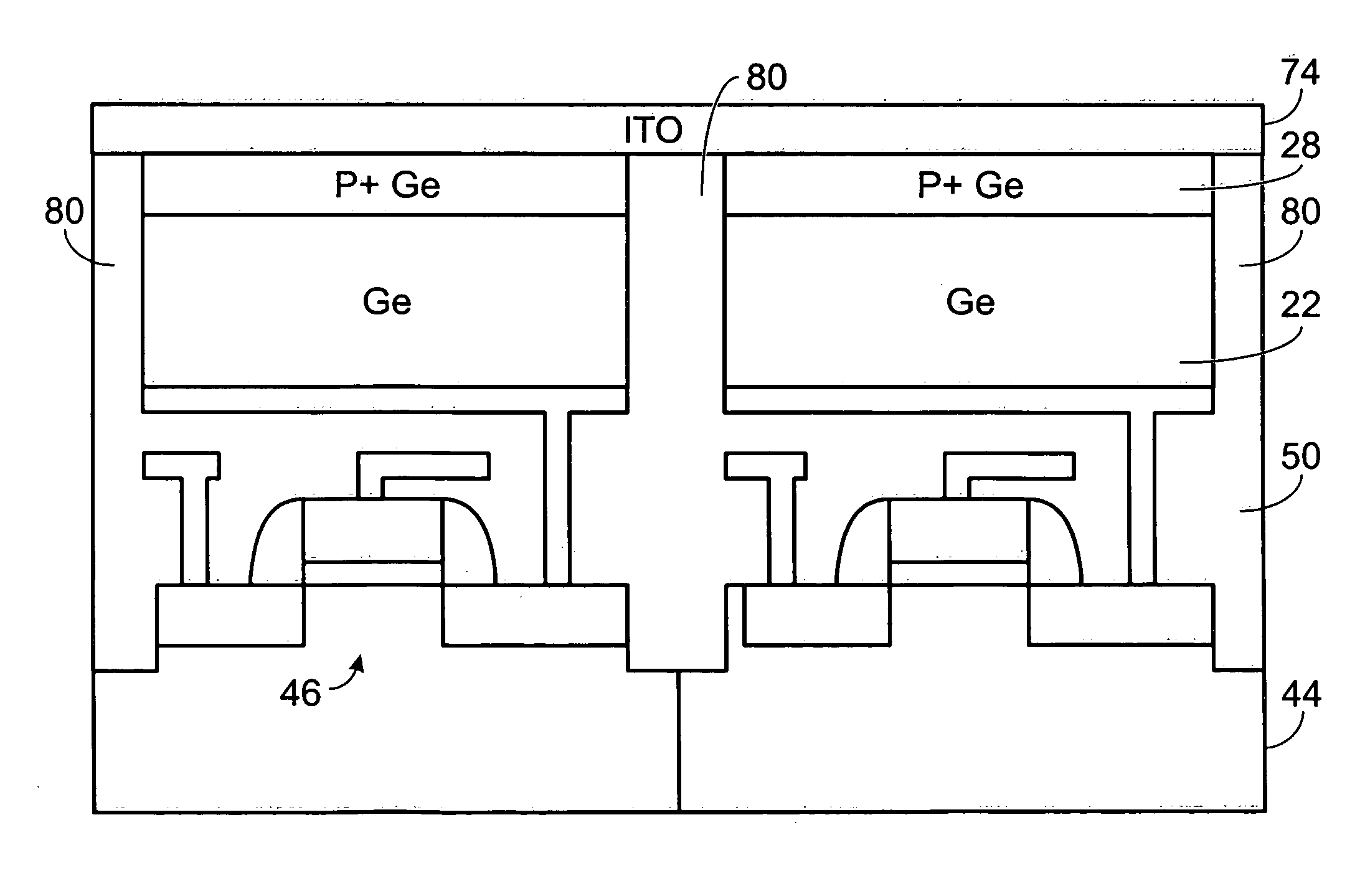
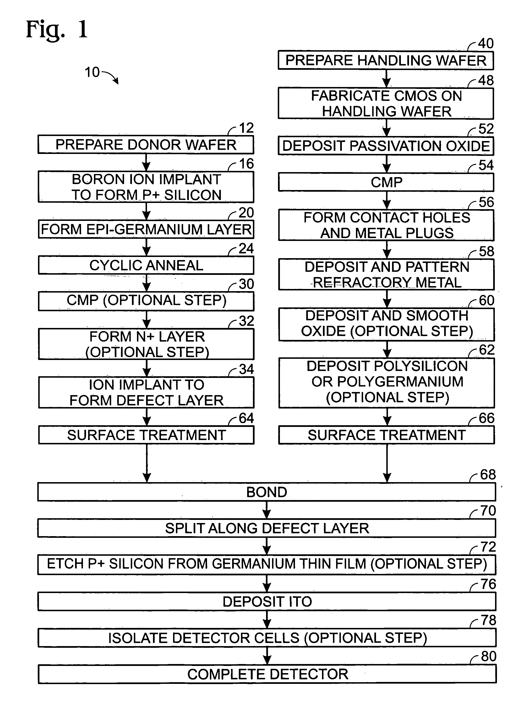
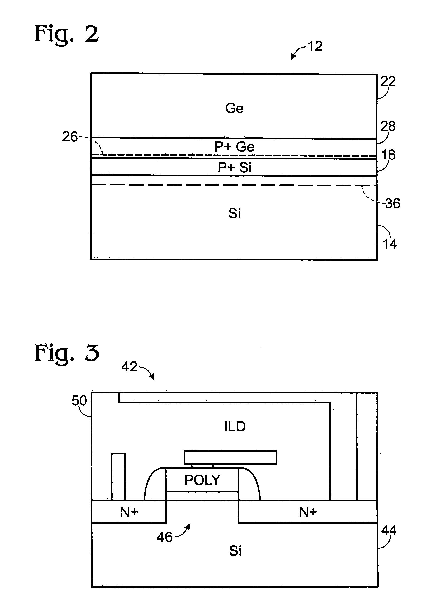
[0013] This disclosure differs from the above-cited U.S. Patent Application in that in the previous disclosure, the germanium wafer is bonded onto a silicon CMOS wafer, and in this disclosure, a germanium thin film is grown onto a silicon donor wafer, followed by a bonding process.

Preparation of Donor Wafers

[0014] Referring now to FIGS. 1 and 2, the initial steps in the method of the invention 10 include preparation of what is referred to herein as a donor wafer 12, including preparation of a convention silicon wafer 14. Ion implantation 16 of boron ions into the silicon wafer converts the surface layer of the donor silicon wafer to a P+ material 18. The doping density is in the order of 1×1019 cm−3 to 1×1020 cm−3.

[0015] The next step is epitaxial growth 20 of between about 0.5 μm to 4.0 μm of germanium 22 onto the P+ wafer material, followed by cyclic annealing 24. The range of temperature for the high temperature portion of the cyclic annealing is between about 800° C. to 900°...


PUM


Abstract

A method of fabricating a germanium infrared sensor for a CMOS imager includes preparation a donor wafer, including: ion implantation into a silicon wafer to form a P+ silicon layer; growing an epitaxial germanium layer on the P+ silicon layer, forming a silicon-germanium interface; cyclic annealing; and implanting hydrogen ions to a depth at least as deep as the P+ silicon layer to form a defect layer; preparing a handling wafer, including: fabricating a CMOS integrated circuit on a silicon substrate; depositing a layer of refractory metal; treating the surfaces of the donor wafer and the handling wafer for bonding; bonding the handling wafer and the donor wafer to form a bonded structure; splitting the bonded structure along the defect layer; depositing a layer of indium tin oxide on the germanium layer; completing the IR sensor.

Description

FIELD OF THE INVENTION [0001] This invention relates to IR sensors, and specifically to fabrication of an IR sensor wherein a germanium thin film is grown on a silicon donor wafer, followed by a bonding and layer transfer process which transfers the germanium layer to another structure. BACKGROUND OF THE INVENTION [0002] Photo detecting in the near-infrared regime, e.g., wavelengths of between about 0.7 μm to 2 μm, has many applications, such as fiber-optical communication, security applications and thermal imaging. Silicon photodiodes are widely used as photodetectors for the visible light regime because of their low dark current and compatibility with silicon integrated circuit technologies. Attempts have been made to deposit Si1-xGex (SiGe) alloys, or germanium thin films, in silicon to fabricate an IR detector, however, the lattice mismatch in a SiGe-to-silicon boundary limits the maximum SiGe thickness which may be formed while still maintaining a defect free structure. Additio...

Claims


Application Information

Patent Timeline
IPC IPC(8): H01L21/30H01L21/46
CPCH01L27/14634H01L27/14649H01L27/14689H01L27/1469H01L31/028H01L31/103H01L31/1804H01L31/1808H01L31/1864Y02E10/547Y02P70/50
Inventor LEE, JONG-JANMAA, JER-SHENHSU, SHENG TENGTWEET, DOUGLAS J.
Owner SHARP KK
Why Eureka
Try Eureka