Plasma nitridization for adjusting transistor threshold voltage

a technology of transistor threshold voltage and plasma nitridization, which is applied in the field of integrated circuit processing, can solve the problems of increasing the threshold voltage, reducing the device dimensions known to decrease the threshold voltage, and undesirable devices with a low threshold voltage, so as to increase the current leakage, convenient operation, and cost-effective

Inactive Publication Date: 2006-08-31
BEAMAN KEVIN L +2
View PDF6 Cites 5 Cited by
  • Summary
  • Abstract
  • Description
  • Claims
  • Application Information

AI Technical Summary

Benefits of technology

[0017] Advantageously, the present invention provides a cost-effective and convenient method of adjusting the voltage of a semiconductor device. Unlike the ion-implantation processes conventionally used to adjust threshold voltage, the nitridization method of the present invention does not involve multiple ion implantation steps and can be conveniently performed using existing equipment and processes in a semiconductor fabrication line. Furthermore, the present method will not cause damages to the crystalline structure of the wafer whereas the traditional processes for threshold voltage adjustment are known to result in crystalline defects which in turn increase current leakage in the P-N junction between the source and the channel region. Furthermore, the present method can be used to conveniently tune the threshold voltage to a desired level without varying the amount of impurities implanted in the semiconductor substrate. These and other objects and advantages of the present invention will become more fully apparent from the following description taken in conjunction with the accompanying drawings.

Problems solved by technology

In particular, impurities in the substrate have shown to increase the threshold voltage, while reduced device dimensions are known to decrease the threshold voltage.
Devices with a low threshold voltage are generally undesirable as they are susceptible to activation by stray currents and other electrical noise.
In particular, transistors having an excessively low threshold voltage are known to be less reliable as they can be inadvertently activated by weak currents emanating from other devices.
On the other hand, transistors with an exceedingly high threshold voltage are also undesirable as a stronger power supply is typically required to effectively operate such devices.
Disadvantageously, however, the ion implantation process is typically expensive and time consuming.
The ion implantation process often results in damage to the crystalline structure of the wafer which can result in leakage currents.
In particular, the ion implantation process entails doping the substrate in a manner that is likely to result in increased current leakage in the P-N junction between the source and the channel region.
Furthermore, such current leakage is known to undesirably affect the performance of a memory circuit as it vitiates the charge carrying capacity of the cell which in turn unfavorably increases the number of refresh times necessary.
Moreover, as device dimensions decrease, it becomes increasingly more difficult to ensure that ions are implanted at the appropriate position within the substrate to obtain the desired effect on threshold voltage.

Method used


Image

  • Plasma nitridization for adjusting transistor threshold voltage
  • Plasma nitridization for adjusting transistor threshold voltage
  • Plasma nitridization for adjusting transistor threshold voltage

Examples


Embodiment Construction

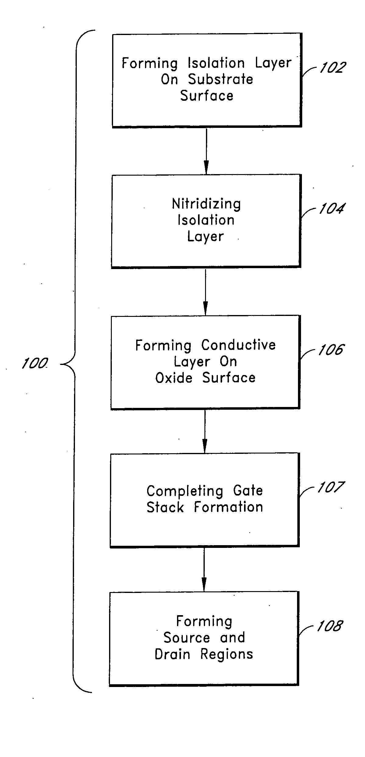
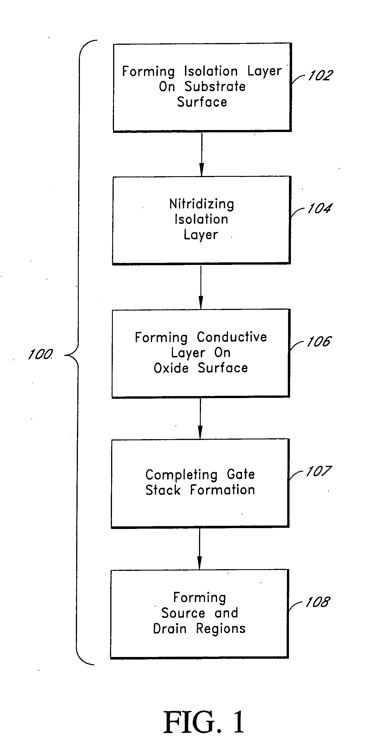
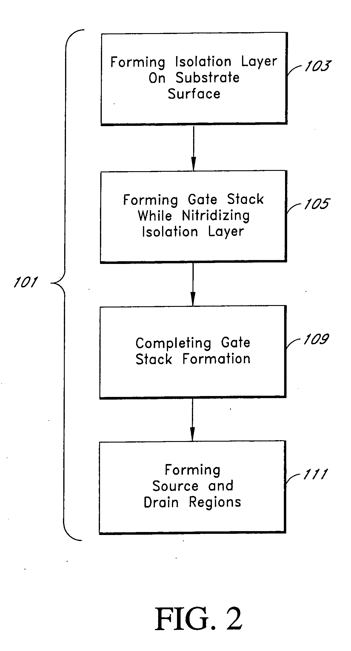
[0026] Reference will now be made to the drawings wherein like numerals refer to like parts throughout. As will be described herein below, the process of the preferred embodiments provides a method of adjusting the transistor threshold voltage by incorporating nitride to the gate oxide layer of the transistor so as to inhibit the mobility of charge carriers in the oxide and thereby increase the threshold voltage required to activate the transistor. As will also be described herein below, the method has also shown to improve gate hardening as well as raising the dielectric constant of the isolation layer, which allows the use of a thinner dielectric layer in semiconductor devices.

[0027]FIG. 1 schematically illustrates a process flow 100 of the preferred embodiment of adjusting the threshold voltage of a transistor using a plasma nitridization process. As shown in FIG. 1, the process begins with a first step 102 comprising the formation of an isolation layer onto a substrate surface....


PUM


Abstract

A method of adjusting the threshold voltage of semiconductor devices by incorporating nitride into the isolation layer so as to decrease the mobility of charge carriers and thereby increase the threshold voltage required to activate the device. The nitrogen incorporation method may comprise of decoupled plasma nitridization (DPN) and the DPN can be performed in-situ during gate oxide formation. The amount of threshold voltage can be varied by adjusting the DPN treatment time and processing parameters.

Description

RELATED APPLICATIONS [0001] This application is a divisional of U.S. patent application Ser. No. 10 / 393,718, filed Mar. 20, 2003, titled “PLASMA NITRIDIZATION FOR ADJUSTING TRANSISTOR THRESHOLD VOLTAGE.”BACKGROUND OF THE INVENTION [0002] 1. Field of the Invention [0003] This invention relates to integrated circuit processing and, more particularly, to a method of adjusting the threshold voltage of transistors using a nitridization process. [0004] 2. Description of the Related Art [0005] The transistor of an integrated circuit typically comprises a source, a drain, and a gate structure that is formed on a substrate surface above the source and the drain. Furthermore, the transistor can be activated by applying a voltage to the gate which in turn creates a conductive channel between the source and the drain in the substrate. When a voltage is applied to the gate through the gate metal, a field effect takes place in the surface of the semiconductor. The effect is either a buildup of ch...

Claims


Application Information

Patent Timeline
Patent Type & Authority Applications(United States)
IPC IPC(8): H01L23/52H01L21/31H01L21/28H01L21/314H01L29/51H01L29/78
CPCH01L21/28061H01L21/28185H01L21/28194H01L21/28211H01L21/3144H01L2924/0002H01L29/518H01L29/78H01L2924/00H01L21/02332H01L21/0234
Inventor BEAMAN, KEVIN L.MOORE, JOHN T.WEIMER, RONALD A.
Owner BEAMAN KEVIN L
Why Eureka
Try Eureka