Compound semiconductor devices and methods of manufacturing the same

Inactive Publication Date: 2006-09-14
LG DISPLAY CO LTD +1
View PDF20 Cites 92 Cited by
  • Summary
  • Abstract
  • Description
  • Claims
  • Application Information

AI Technical Summary

Benefits of technology

[0011] In one embodiment, the compound semiconductor device may further comprise a buffer layer disposed between the substrate and the compound semiconductor thin film in order to minimize the density of crystal defects in the compound semiconductor thin film by reducing a crystalline difference between the substrate and the compound semiconductor thin film. In a related embodimen

Problems solved by technology

However, it is not easy to fabricate a GaN single-crystalline substrate.
Because GaN solid has a very high melting point (72000° C.) and/or can decompose into Ga and N2 before it melts, GaN crystals cannot be made using a typical Czochralski technique for growing crystals from a solution.
Although it may

Method used


Image

  • Compound semiconductor devices and methods of manufacturing the same
  • Compound semiconductor devices and methods of manufacturing the same
  • Compound semiconductor devices and methods of manufacturing the same

Examples


embodiment 1

[0026]FIGS. 3 through 7 are cross-sectional views illustrating a compound semiconductor device and method of manufacturing the same according to a first exemplary embodiment.

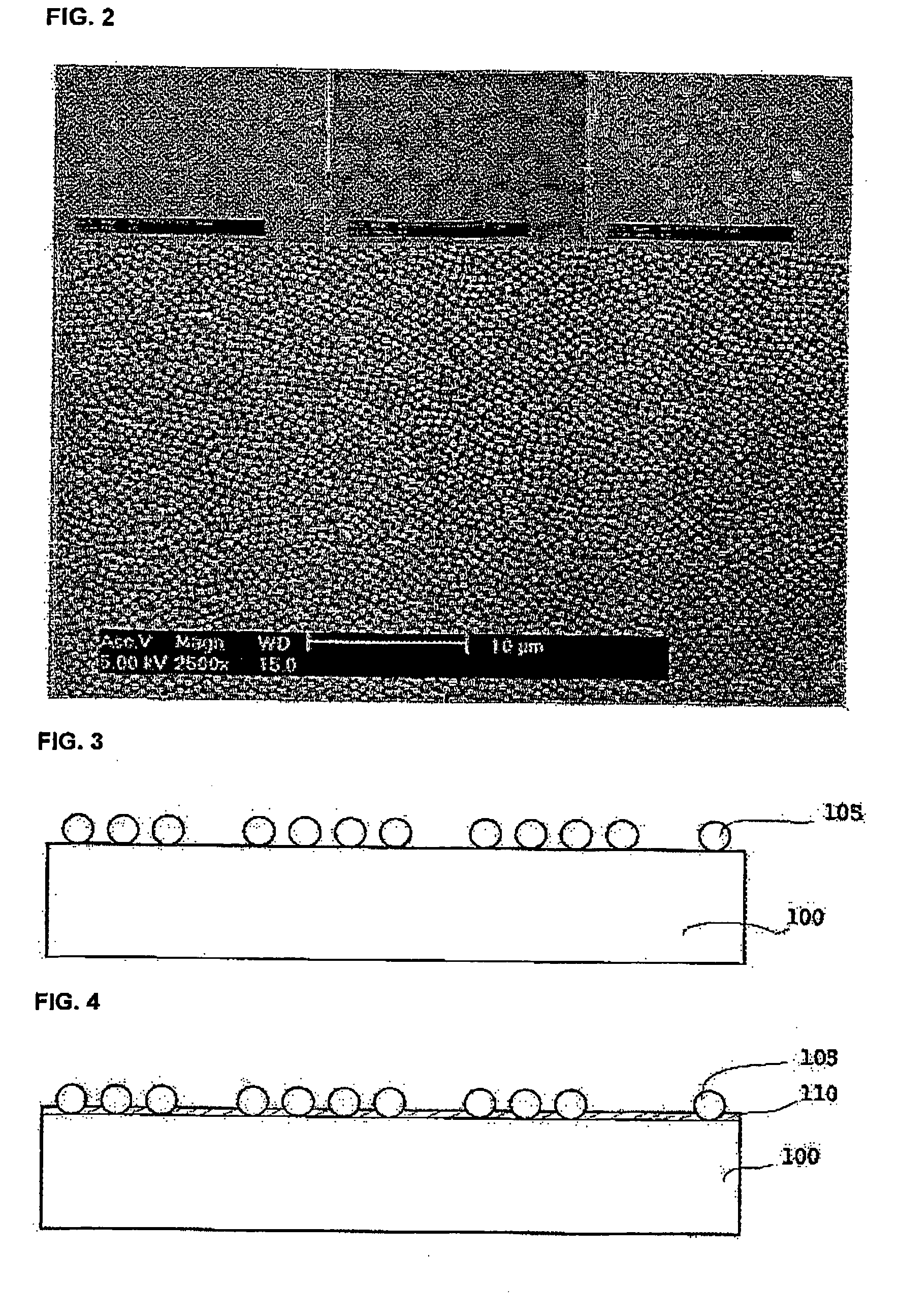
[0027] Referring to FIG. 3, a plurality of spherical balls 105 are made and coated on a substrate 100. The spherical balls 105 may be formed of SiO2, Al2O3, TiO2, ZrO2, Y2O3—ZrO2, CuO, Cu2O, Ta2O5, PZT(Pb(Zr, Ti)O3), Nb2O5, FeSO4, Fe3O4, Fe2O3, Na2SO4, GeO2, CdS, or a metal. For example, to make SiO2 spherical balls, a first solution is made by dissolving tetraethylorthosilicate (TEOS) in anhydrous ethanol. An ammonia ethanol solution is mixed with deionized water and ethanol, thus making a second solution. Ammonia acts as a catalyst for making the spherical balls 105. The first solution is mixed with the second solution, and the mixture of the first and second solutions is stirred at a predetermined temperature for a predetermined amount of time. The spherical balls 105 are separated from the stirred mixture u...

embodiment 2

[0043]FIG. 8 is a cross-sectional view illustrating a compound semiconductor thin film and method of manufacturing the same according to a second exemplary embodiment.

[0044] Referring to FIG. 8, the processes described with reference to FIGS. 3 through 6 are performed to form a compound semiconductor thin film. That is, spherical balls 205 are made and coated on a substrate 200, a buffer layer 210 is grown, and a compound semiconductor thin film 215 is grown between the spherical balls 205 on the buffer layer 210.

[0045] The substrate 200 having the compound semiconductor thin film 215 is taken out of a reactor. Thereafter, spherical balls 220 with a size of several nm to several tens of μm are coated on the first compound semiconductor thin film 215. Next, the substrate 200 having the spherical balls 220 is loaded again into the reactor, and a second compound semiconductor thin film 225 is grown on the first compound semiconductor thin film 215 having the spherical balls 220.

embodiment 3

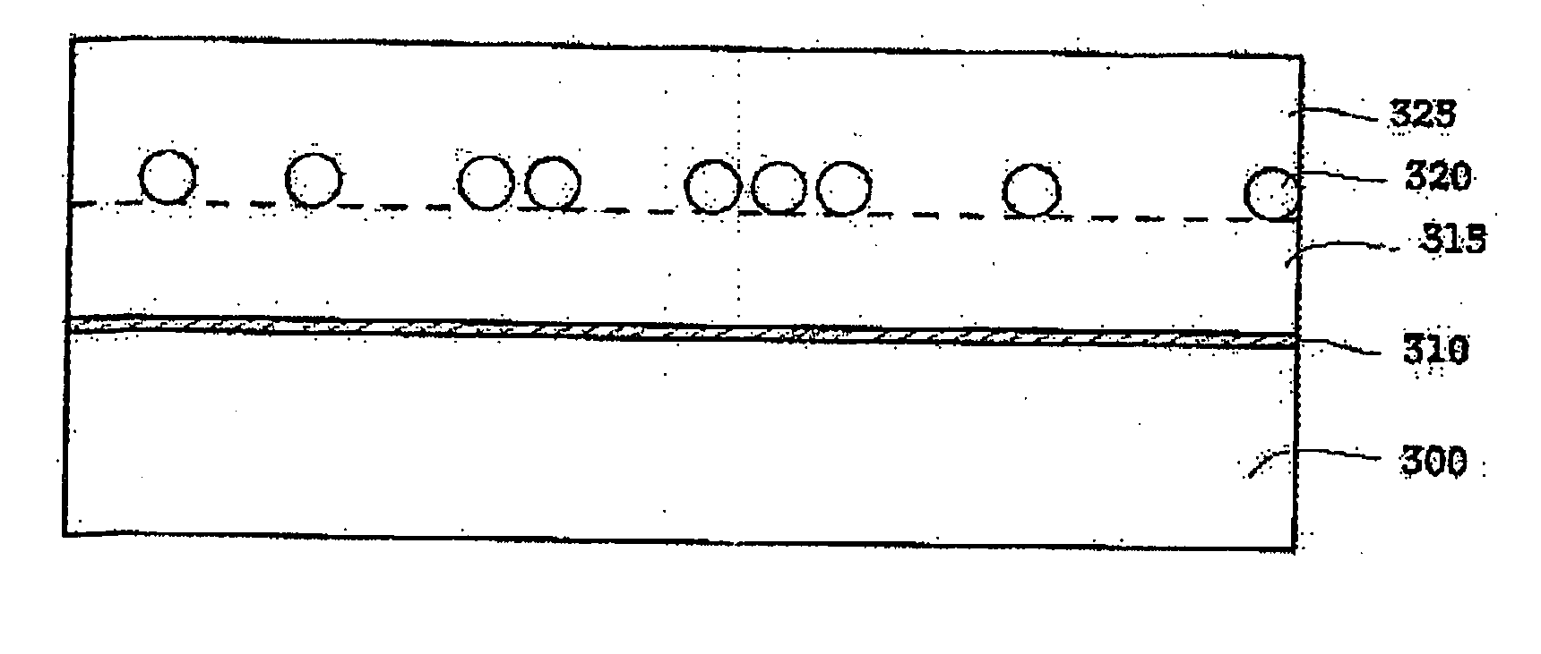
[0046]FIG. 9 is a cross-sectional view illustrating a compound semiconductor device and method of manufacturing the same according to a third exemplary embodiment.

[0047] Referring to FIG. 9, the processes described with reference to FIGS. 4 through 6 are performed, thus a buffer layer and a compound semiconductor thin film are grown on a substrate. That is, a buffer layer 310 is grown on a substrate 300, and then a compound semiconductor thin film 315 is grown on the buffer layer 310.

[0048] The substrate 300 on which the compound semiconductor thin film 315 is formed is unloaded from a reactor. Thereafter, spherical balls 320 with a size of several nm to several tens of μm are coated on the compound semiconductor thin film 315 in the same manner as described with reference to FIG. 3, and a compound semiconductor thin film 325 is grown on the compound semiconductor thin film 315 on which the spherical balls 320 are coated.

[0049] Like in the above embodiments, the method of growing...


PUM


Abstract

A compound semiconductor device and method of manufacturing the same. The method includes coating a plurality of spherical balls on a substrate and selectively growing a compound semiconductor thin film on the substrate on which the spherical balls are coated. The entire process can be simplified and a high-quality compound semiconductor thin film can be grown in a short amount of time in comparison to an epitaxial lateral overgrowth (ELO) method.

Description

BACKGROUND [0001] 1. Technical Field [0002] Compound semiconductor devices are disclosed which have a compound semiconductor thin film grown on a substrate on which spherical balls are coated. Methods of manufacturing the same are also disclosed. [0003] 2. Description of the Related Art [0004] Gallium nitride (GaN) is known as a material that is useful for blue light-emitting devices or high-temperature electronic devices. However, it is not easy to fabricate a GaN single-crystalline substrate. Because GaN solid has a very high melting point (72000° C.) and / or can decompose into Ga and N2 before it melts, GaN crystals cannot be made using a typical Czochralski technique for growing crystals from a solution. Although it may be possible to form a GaN solution by applying an ultra-high voltage to the GaN solid, this method becomes problematic in terms of mass production. [0005] Because of the increased demand for light emitting devices that emit blue wavelength light, nitride (or GaN-b...

Claims


Application Information

Patent Timeline
IPC IPC(8): H01L31/00H01L21/3205H01L29/739H01L21/4763C30B25/18C30B29/38H01L21/205H01L33/32H01S5/323
CPCH01L21/0237H01L21/02458H01L21/02502H01L21/0254H01L21/0262H01L21/02639H01L21/02642H01L31/0296H01L31/035281H01L33/007H01L33/12G03G21/1814G03G2221/183
Inventor YI, GYU-CHULAN, SUNG-JINKIM, YONG-JINLEE, DONG-KUN
Owner LG DISPLAY CO LTD
Why Eureka
Try Eureka