Non-volatile memory and method with power-saving read and program-verify operations

a non-volatile memory and program verification technology, applied in static storage, digital storage, instruments, etc., can solve the problems of unsuitable mobile and handheld environment, prone to mechanical failure, and bulky disk drives, and achieve the effect of eliminating the power-consuming charging and discharging of those bit lines

Active Publication Date: 2006-09-21
SANDISK TECH LLC
View PDF49 Cites 123 Cited by
  • Summary
  • Abstract
  • Description
  • Claims
  • Application Information

AI Technical Summary

Benefits of technology

[0042] The saving in power by the various aspects of the present invention allows for a more power efficient memory device. The saving in power consumption can amount to as much as fifty percent as compared to existing read / write circuits. In particular, a larger number of read / write modules can be used in parallel without requiring a bulky power supply.
[0044] In one embodiment, at least a subset of the undischarged bit lines will retain its voltage when cycling between alternate program and verify phases, thereby eliminating the power-consuming charging and discharging of those bit lines in every program phase. The subset of the undischarged bit line corresponds to memory cells that have been verified relative to a current demarcation threshold voltage.
[0045] In another embodiment, all the undischarged bit lines will retain it voltage when cycling between alternate program and verify phases, thereby eliminating the power-consuming charging and discharging of those bit lines in every program phase. This is accomplished by preventing the lockout bit lines to be discharged by their conducting cells. A switch is provided between each memory cell or NAND chain and its associated bit line. The switch is responsive to a voltage condition on its associated bit line to connect the memory cell or NAND chain to its associated bit line when the bit line is substantially at zero voltage and to disconnect the memory cell or NAND chain from its associated bit line when the bit line is substantially at a supply voltage.

Problems solved by technology

Conventional mass storage, based on rotating magnetic medium such as hard drives and floppy disks, is unsuitable for the mobile and handheld environment.
This is because disk drives tend to be bulky, are prone to mechanical failure and have high latency and high power requirements.
These undesirable attributes make disk-based storage impractical in most mobile and portable applications.
It is often difficult to perform both of these functions in an optimum manner with a single voltage.
Programming of charge storage memory devices can only result in adding more charge to its charge storage elements.
However, the interleaving page architecture is disadvantageous in at least three respects.
First, it requires additional multiplexing circuitry.
Secondly, it is slow in performance.
Thirdly, it is also not optimum in addressing other disturb effects such as field coupling between neighboring charge storage elements at the floating gate level when the two neighbors are programmed at different times, such as separately in odd and even pages.
However, sensing all bit lines does bring up the problem of cross-talk between neighboring bit lines due induced currents from their mutual capacitance.
With the bit line voltage clamped, the conventional method of sensing the discharge due to the bit line capacitance can not be applied.
The power consumption is even more acute for the all-bit-line architecture where there is potentially twice the number of memory cells operating in parallel than that of the alternate bit-line architecture.

Method used


Image

  • Non-volatile memory and method with power-saving read and program-verify operations
  • Non-volatile memory and method with power-saving read and program-verify operations
  • Non-volatile memory and method with power-saving read and program-verify operations

Examples


Embodiment Construction

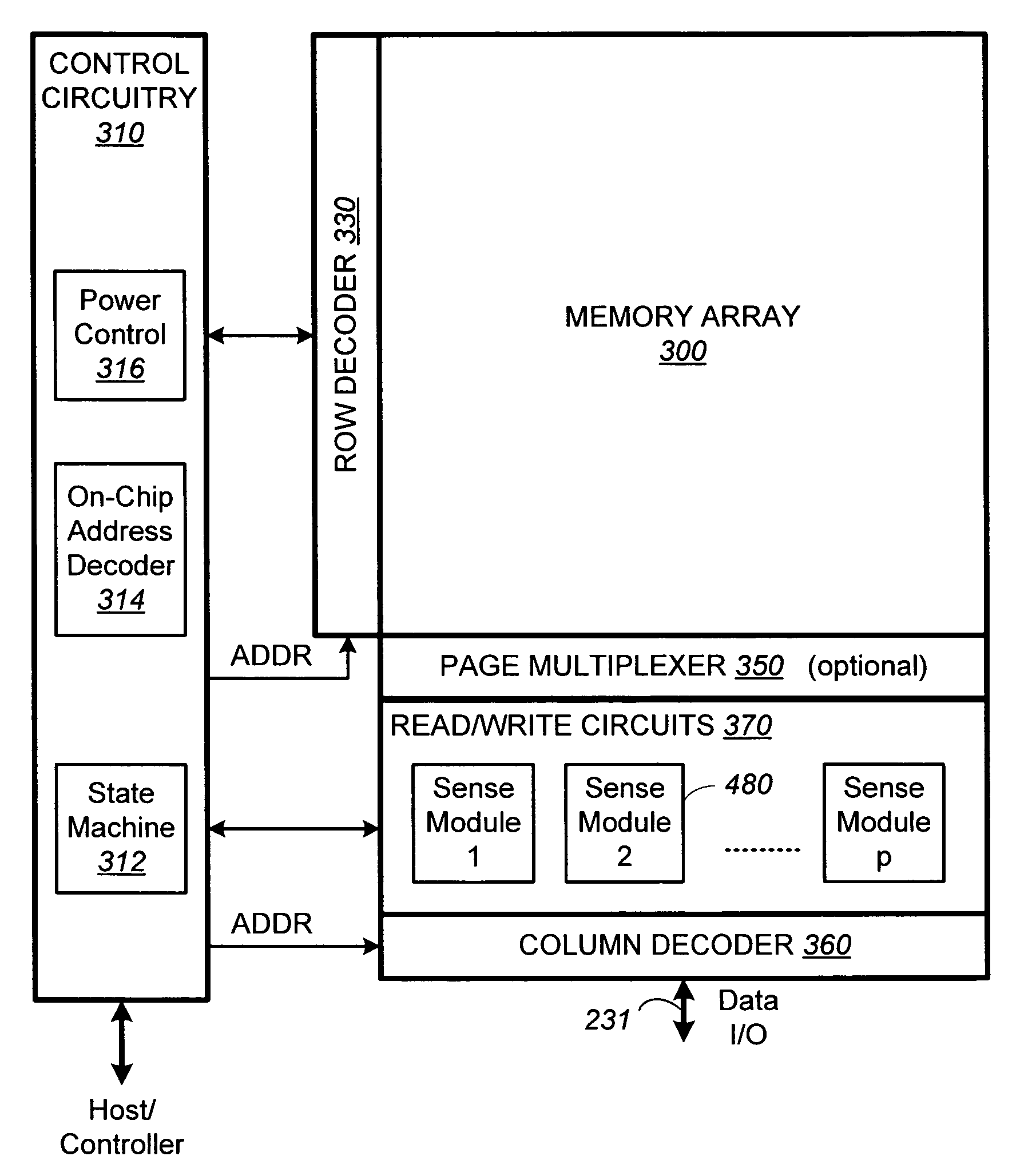
[0083]FIG. 6A illustrates schematically a compact memory device having a bank of read / write circuits, which provides the context in which the present invention is implemented. The memory device includes a two-dimensional array of memory cells 300, control circuitry 310, and read / write circuits 370. The memory array 300 is addressable by word lines via a row decoder 330 and by bit lines via a column decoder 360. The read / write circuits 370 is implemented as a bank of sense modules 480 and allows a block (also referred to as a “page”) of memory cells to be read or programmed in parallel. In a preferred embodiment, a page is constituted from a contiguous row of memory cells. In another embodiment, where a row of memory cells are partitioned into multiple blocks or pages, a block multiplexer 350 is provided to multiplex the read / write circuits 370 to the individual blocks.

[0084] The control circuitry 310 cooperates with the read / write circuits 370 to perform memory operations on the me...


PUM


Abstract

A non-volatile memory device capable of reading and writing a large number of memory cells with multiple read / write circuits in parallel has features to reduce power consumption during read, and program / verify operations. A read or program verify operation includes one or more sensing cycles relative to one or more demarcation threshold voltages to determine a memory state. In one aspect, selective memory cells among the group being sensed in parallel have their conduction currents turned off when they are determined to be in a state not relevant to the current sensing cycle. In another aspect, a power-consuming period is minimized by preemptively starting any operations that would prolong the period. In a program / verify operation cells not to be programmed have their bit lines charged up in the program phase. Power is saved when a set of these bit lines avoids re-charging at every passing of a program phase.

Description

FIELD OF THE INVENTION [0001] This invention relates generally to non-volatile semiconductor memory such as electrically erasable programmable read-only memory (EEPROM) and flash EEPROM, and specifically ones implementing power-saving features during read and program verify operations. BACKGROUND OF THE INVENTION [0002] Solid-state memory capable of nonvolatile storage of charge, particularly in the form of EEPROM and flash EEPROM packaged as a small form factor card, has recently become the storage of choice in a variety of mobile and handheld devices, notably information appliances and consumer electronics products. Unlike RAM (random access memory) that is also solid-state memory, flash memory is non-volatile, retaining its stored data even after power is turned off. In spite of the higher cost, flash memory is increasingly being used in mass storage applications. Conventional mass storage, based on rotating magnetic medium such as hard drives and floppy disks, is unsuitable for ...

Claims


Application Information

Patent Timeline
Patent Type & Authority Applications(United States)
IPC IPC(8): G11C16/04
CPCG11C11/5642G11C2211/5621G11C16/26G11C16/34
Inventor LI, YANLEE, SEUNGPILCHAN, SIU LUNG
Owner SANDISK TECH LLC
Why Eureka
Try Eureka