Baffle wafers and randomly oriented polycrystalline silicon used therefor

Active Publication Date: 2006-09-21
HANGZHOU DUNYUANJUXIN SEMICON TECH CO LTD
View PDF10 Cites 28 Cited by
  • Summary
  • Abstract
  • Description
  • Claims
  • Application Information

AI Technical Summary

Benefits of technology

[0016] The baffle wafer may be prepared in a multi-step process. After being cut from the ingot, the wafer may be etched, for example, in an alkaline solution to reduce or eliminate strain. The wafer, preferably after strain etching, is subject to surface treatment producing sub-surface damage on its two principal surfaces and perhaps on its peripheral edge. The sub-surface damage may be performed by bead blasting or by grinding or machining. The surface-damaged wafer is then subjected to an acidic cleaning step and then to ultrasonic cleaning.
[0017] CZ grown or randomly oriented polysilicon is also useful for forming machined structures because of its purity, fine polycrystalline structure, and ruggedness.

Problems solved by technology

The wafer, preferably after strain etching, is subject to surface treatment producing sub-surface damage on its two principal surfaces and perhaps on its peripheral edge.

Method used


Image

  • Baffle wafers and randomly oriented polycrystalline silicon used therefor
  • Baffle wafers and randomly oriented polycrystalline silicon used therefor
  • Baffle wafers and randomly oriented polycrystalline silicon used therefor

Examples


Embodiment Construction

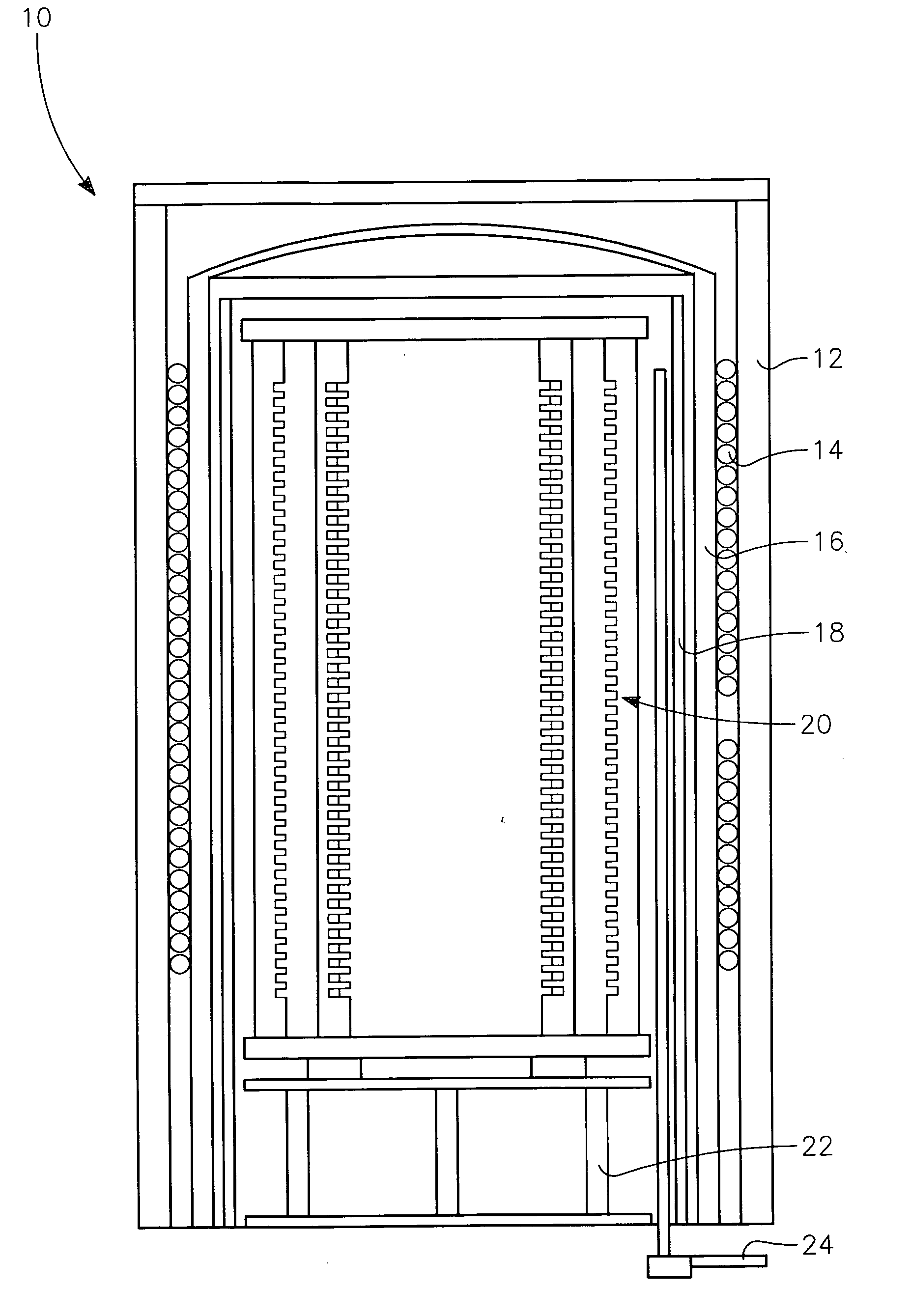
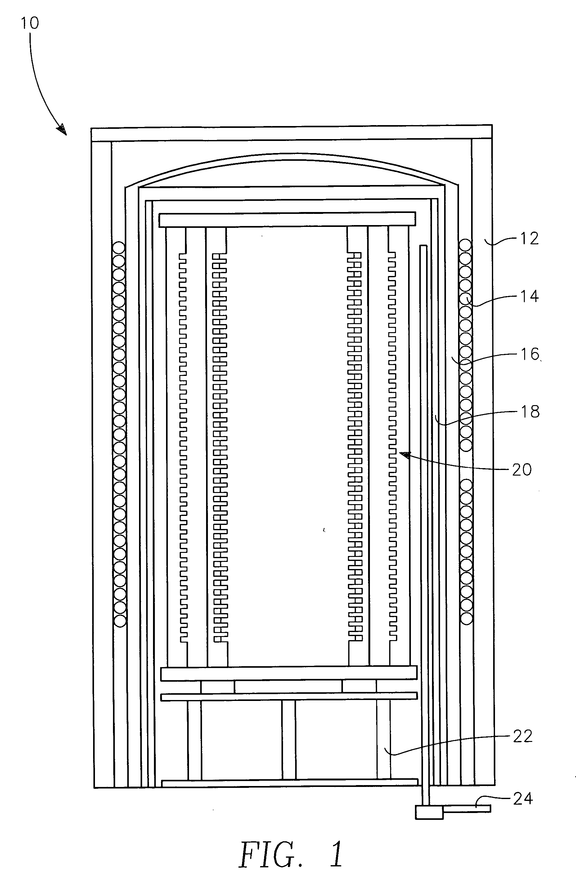
[0029] We believe that commercial grade silicon production wafers are inappropriate for use as buffer and dummy wafers, collectively referred to as baffle wafers, because they are monocrystalline. It is understood that production wafers often are not perfectly monocrystalline and may have several defects including dislocations and slips. However, the defects must be minimal for reasonable yield in production and the typical goal is to obtain and maintain low-dislocation and slip-free monocrystalline production wafers.

[0030] If the edge of the monocrystalline wafer is chipped under repeated usage as a baffle wafer, the crack is likely to propagate across the wafer along crystalline cleavage planes and cause it to break. Commercial grade monocrystalline wafers are further inappropriate for baffle wafers because they are expensive. Although older wafers were surface treated on their back side while their front surfaces were polished, very advanced production has required polishing on ...


PUM

PropertyMeasurementUnit
Size distributionaaaaaaaaaa
Diameteraaaaaaaaaa

Abstract

Baffle wafers of polycrystalline silicon are placed in non-production slots of a support tower for thermal processing monocrystalline silicon wafers. The polycrystalline silicon is preferably randomly oriented Czochralski polysilicon grown using a randomly oriented seed, for example, CVD grown silicon. An all-silicon hot zone of a thermal furnace may include a silicon support tower placed within a silicon liner and supporting the polysilicon baffle wafers with silicon injector tube providing processing gas within the liner. The randomly oriented polysilicon may be used for other parts requiring a rugged member, for example, within a silicon processing chamber and for structural members.

Description

RELATED APPLICATION [0001] This application claims benefit of provisional application 60 / 658,075 filed Mar. 3, 2005 and provisional application 60 / 694,334 filed Jun. 27, 2005.FIELD OF THE INVENTION [0002] The invention relates generally to thermal processing of silicon wafers. In particular, it relates to non-production wafers used in batch thermal processing of production wafers. The invention also relates to a form of polycrystalline silicon useful for such non-production wafers as well as for other uses. BACKGROUND ART [0003] Batch thermal processing continues to be used for several stages of fabrication of silicon integrated circuits. One low temperature thermal process deposits a layer of silicon nitride by chemical vapor deposition, typically using chlorosilane and ammonia as the precursor gases at temperatures in the range of about 700° C. Other, high-temperature processes include oxidation, annealing, silicidation, and other processes typically using higher temperatures, for...

Claims


Application Information

Patent Timeline
IPC IPC(8): H01L21/30H01L21/46
CPCC30B15/00C30B29/06Y10T428/24355H01L21/673C30B33/02
Inventor BOYLE, JAMES E.REYNOLDS, REESEZEHAVI, RANAAN Y.MYTTON, ROBERT W.CADWELL, TOM L.
Owner HANGZHOU DUNYUANJUXIN SEMICON TECH CO LTD
Why Eureka
Try Eureka