Semiconductor device and method of manufacturing semiconductor device

a semiconductor device and semiconductor technology, applied in the direction of semiconductor devices, electrical devices, transistors, etc., can solve the problems of insufficient improvement of complicated mask pattern for use in the photolithography process, so as to achieve the effect of improving the performance of the semiconductor devi

Inactive Publication Date: 2006-09-28
RENESAS TECH CORP
View PDF0 Cites 91 Cited by
  • Summary
  • Abstract
  • Description
  • Claims
  • Application Information

AI Technical Summary

Benefits of technology

[0009] An object of the present invention is to provide a technique of achieving improved performance of a semiconductor device including a plurality of MOS transistors.

Problems solved by technology

Therefore, even when the technique disclosed in the above-mentioned JP2003-124463 is applied to the MOS transistors in the logic circuit area, advantages of the double- or tri-gate structure might not be exercised sufficiently depending on MOS transistors to be used.
This causes problems such as an insufficient improvement in performance of the semiconductor device.
However, to design a plurality of MOS transistors to have different gate widths, active regions in which the plurality of MOS transistors are to be formed need to have different widths, which results in a complicated mask pattern for use in a photolithography process.
As a result, a sufficient process margin for the photolithography process may not be secured, and hence, the performance of the semiconductor device may not be secured sufficiently.

Method used


Image

  • Semiconductor device and method of manufacturing semiconductor device
  • Semiconductor device and method of manufacturing semiconductor device
  • Semiconductor device and method of manufacturing semiconductor device

Examples


first preferred embodiment

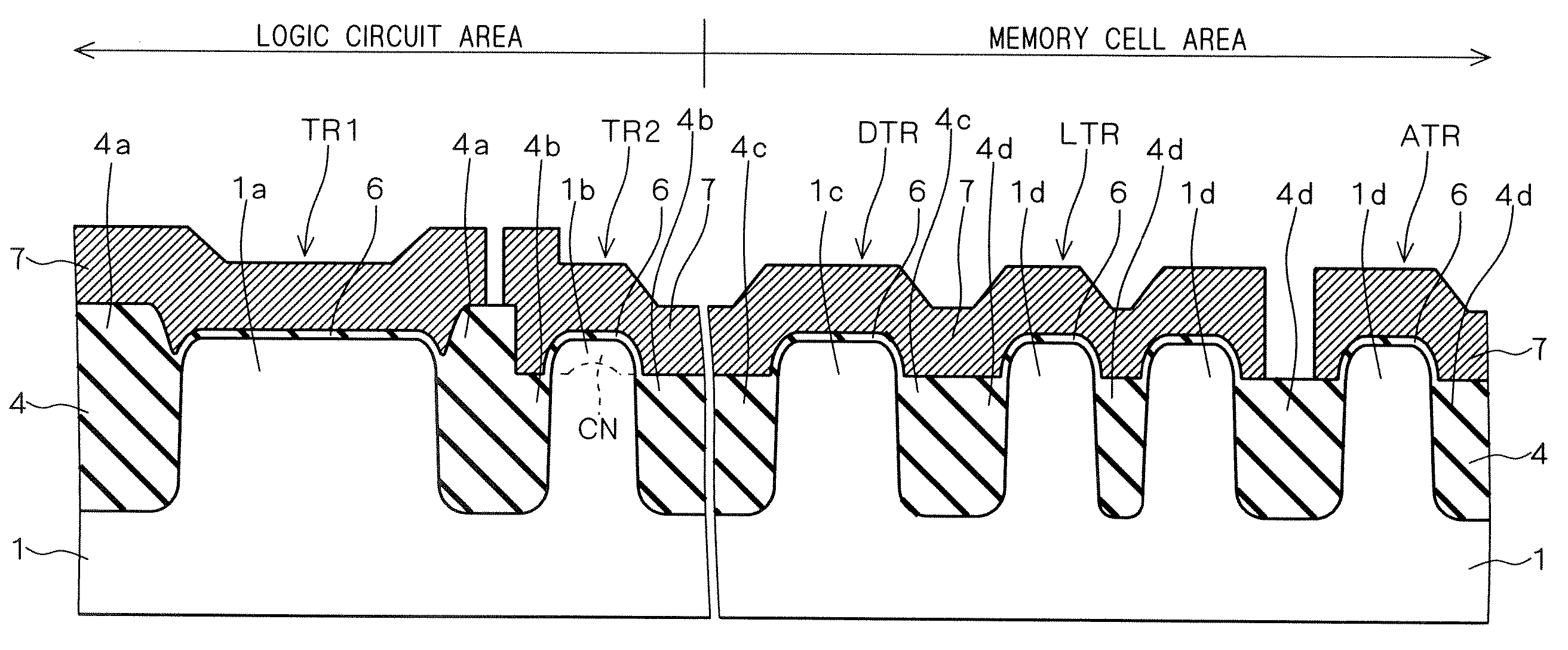
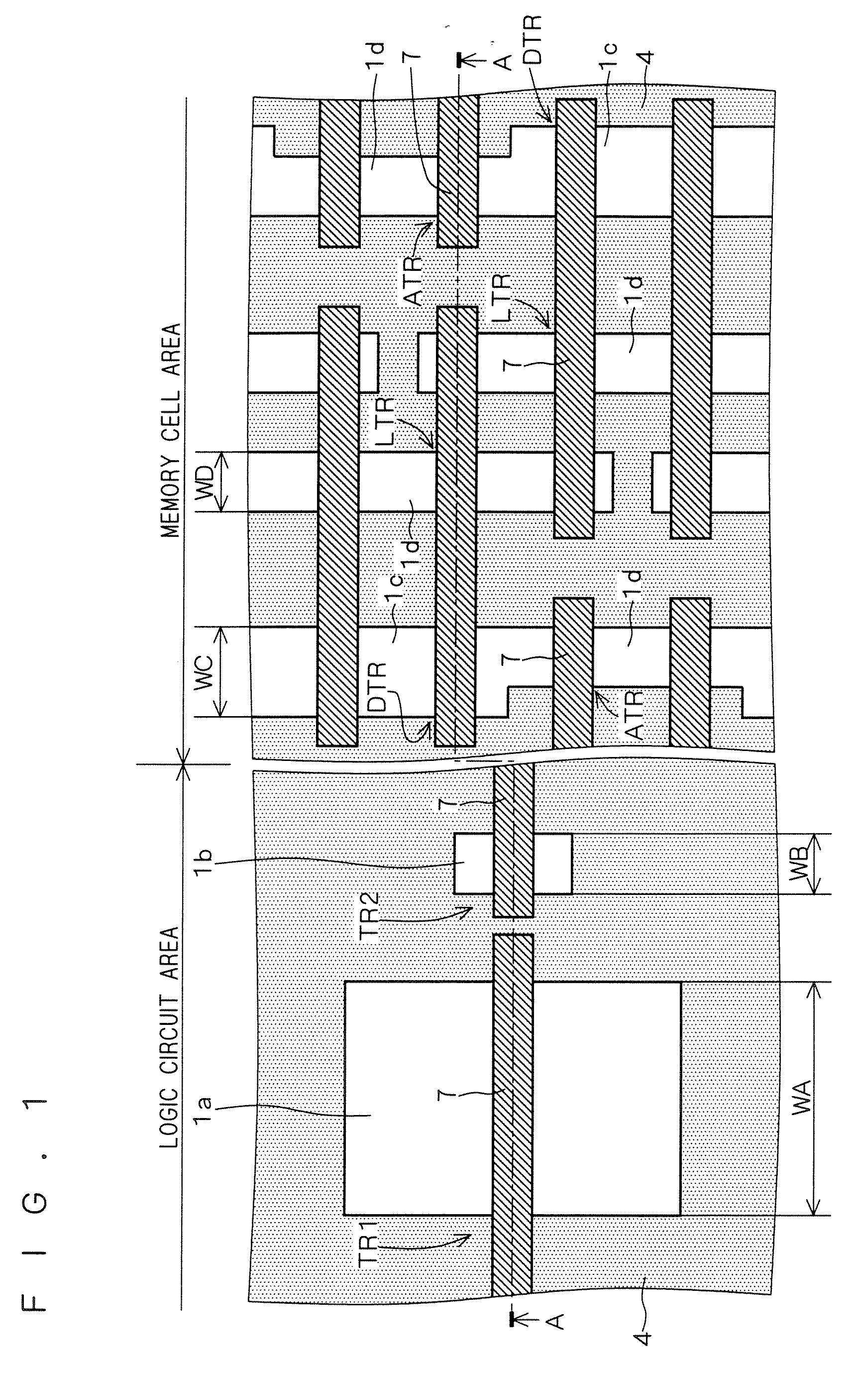
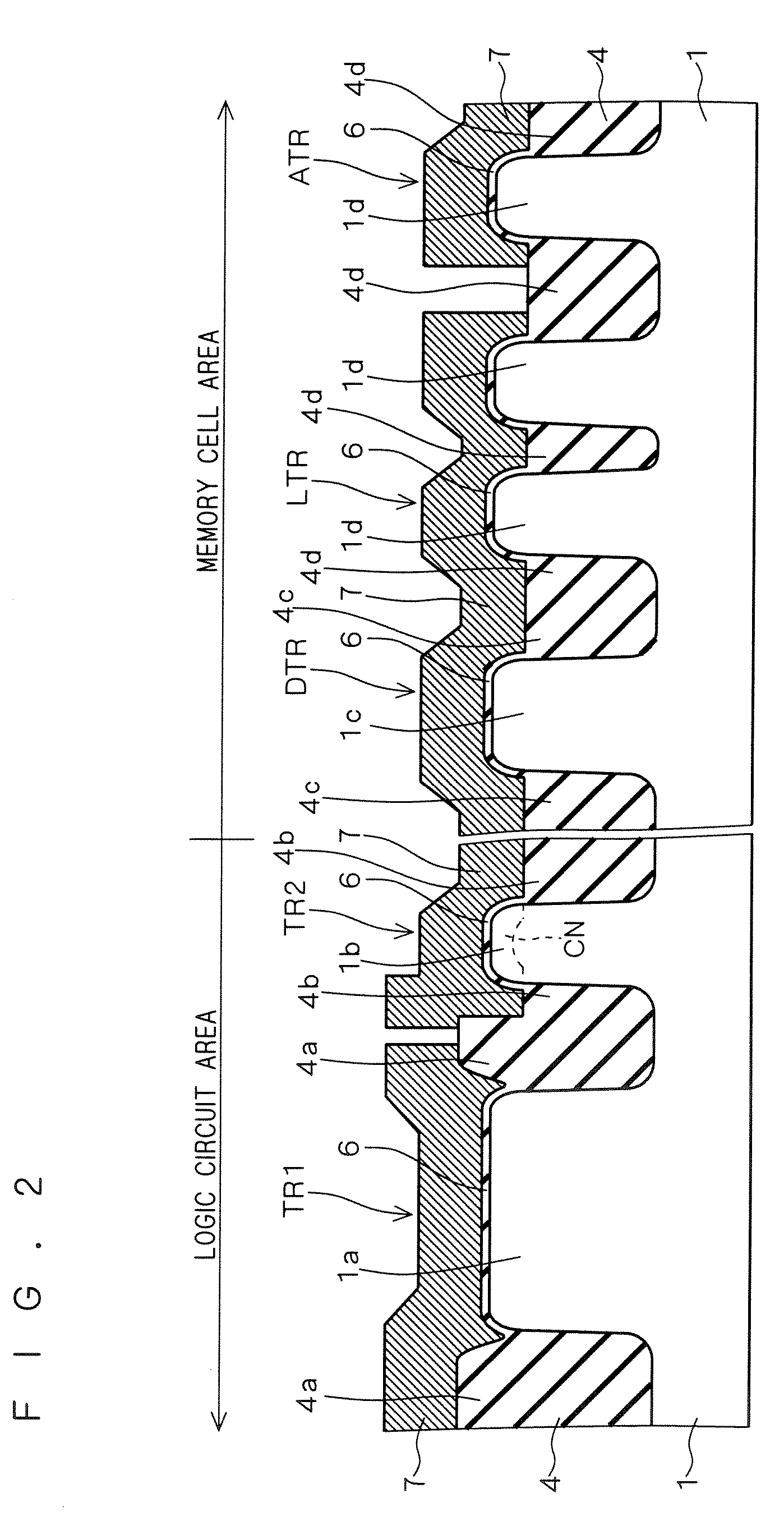
[0030]FIG. 1 is a plan view showing the structure of a semiconductor device according to a first preferred embodiment of the present invention, and FIG. 2 is a sectional view taken along the line A-A in FIG. 1. FIG. 3 is a circuit diagram of a memory cell provided in the semiconductor device according to the present embodiment.

[0031] The semiconductor device according to the present embodiment has a logic circuit area in which a logic circuit is formed and a memory cell area in which a plurality of memory cells are formed. For example, the semiconductor device has a logic circuit for performing data processing on image data or communication data and eSRAM (embedded SRAM). In the memory cell area, a plurality of memory cells in eSRAM, for example, are arranged in an array. In the logic circuit area, a peripheral circuit including column and row decoders for driving the plurality of memory cells and a logic circuit other than the peripheral circuit for processing image data or commun...

second preferred embodiment

[0078]FIG. 23 is a plan view showing the structure of a semiconductor device according to a second preferred embodiment of the invention. FIG. 24 is a sectional view taken along the line C-C shown in FIG. 23. The semiconductor device according to the present embodiment differs from that of the first preferred embodiment in the width WC of the active region 1c as viewed from above and the height of the peripheral portion 4c in the isolation insulation film 4.

[0079] In the present embodiment, as shown in FIG. 23, the width WC of the active region 1c is equal to the width WD of the active region 1d as viewed from above. Accordingly, in the present embodiment, the width WB of the active region 1b, width WC of the active region 1c and width WD of the active region 1d are equal to one another, and smaller than the width WA of the active region 1a. The widths WB to WD of the active regions 1b to 1d are set not greater than 50 nm, and preferably at 20 to 50 nm from a manufacturability stan...


PUM


Abstract

First active region and second and third active regions are defined in a semiconductor substrate within a memory cell area and a logic circuit area, respectively. First to third MOS transistors are formed in the first to third active regions, respectively. As viewed from above, the length of the first and second active regions along the gate width is not greater than the length of the third active region along the gate width. In the isolation insulation film, the upper surface of a peripheral portion provided around the first active region is positioned below the upper surface thereof, and the upper surface of a peripheral portion provided around the second active region is positioned below the upper surface thereof. A gate electrode is formed on the upper surfaces of the first to third active regions and the side surfaces of the first and second active regions.

Description

BACKGROUND OF THE INVENTION [0001] 1. Field of the Invention [0002] The present invention relates to a semiconductor device including a plurality of MOS transistors and a method of manufacturing the semiconductor device. [0003] 2. Description of the Background Art [0004] Gate structures called the double-gate structure and the tri-gate structure have conventionally been proposed for achieving improved turn-on and turn-off characteristics of MOS transistors. Such gate structures have a gate electrode surrounding, from multiple directions, a semiconductor area in which a channel region for a MOS transistor is to be formed, thereby achieving improved controllability of the channel region by a gate voltage. [0005] For instance, Fu-Liang Yang et al., “35 nm CMOS FinFETs” (2002 Symposium on VLSI Technology Digest of Technical Papers, p. 104) and Fu-Liang Yang et al., “5 nm-Gate Nanowire FinFETs” (2004 Symposium on VLSI Technology Digest of Technical Papers, p. 196) disclose a double-gate ...

Claims


Application Information

Patent Timeline
Patent Type & Authority Applications(United States)
IPC IPC(8): H01L29/94
CPCH01L27/0207H01L27/105H01L27/11H01L27/1104H01L27/1116H01L29/7851H01L29/7854H10B10/18H10B10/00H10B10/12
Inventor HORITA, KATSUYUKIISHIBASHI, MASATO
Owner RENESAS TECH CORP
Why Eureka
Try Eureka