Display device

a display device and display technology, applied in non-linear optics, instruments, optics, etc., can solve the problems of large stray capacitance value, difficult positioning relationship with tft substrate, and complicated circuits, and achieve high operational margin, low cost, and high reliability

Active Publication Date: 2006-09-28
NEC LCD TECH CORP
View PDF3 Cites 41 Cited by
  • Summary
  • Abstract
  • Description
  • Claims
  • Application Information

AI Technical Summary

Benefits of technology

[0051] As described above, according to the present invention, a circuit element, in a driver circuit for controlling pixels in a display area, affected by stray capacitance formed between a conductive seal and a driver circuit is disposed apart from the conductive seal. Thereby, even if voltage fluctuation of counter electrode is caused, it is possible to prevent an influence placed by the stray capacitance on the driver circuit, whereby high operational margin and high reliability can be secured. Further, since it has such a configuration that only positional relationship of the circuit element to the conductive seal is changed, it is possible to a...

Problems solved by technology

Further, some conventional driving circuit integrated-type liquid crystal display devices consisting of polysilicon TFT, are so formed that more complicated circuits such as DAC circuits are integrated.
Therefore, in order to incorporate a driving circuit into the TFT substrate without interfering the function of the TFT substrate, positioning relationship with the TFT substrate becomes a problem.
Therefore, the stray capacitance value of the stray capacitance is very large.
Therefore, since the fluctuation value becomes large necessarily, the problem becomes prominent.
Therefore, as potential of the floating node varies according to the fluctuation of Vcom, there may be caused an operational error, or a decrease in circuit operational margin even operational error is not caused, or a decrease in re...

Method used


Image

  • Display device
  • Display device
  • Display device

Examples


embodiment 1

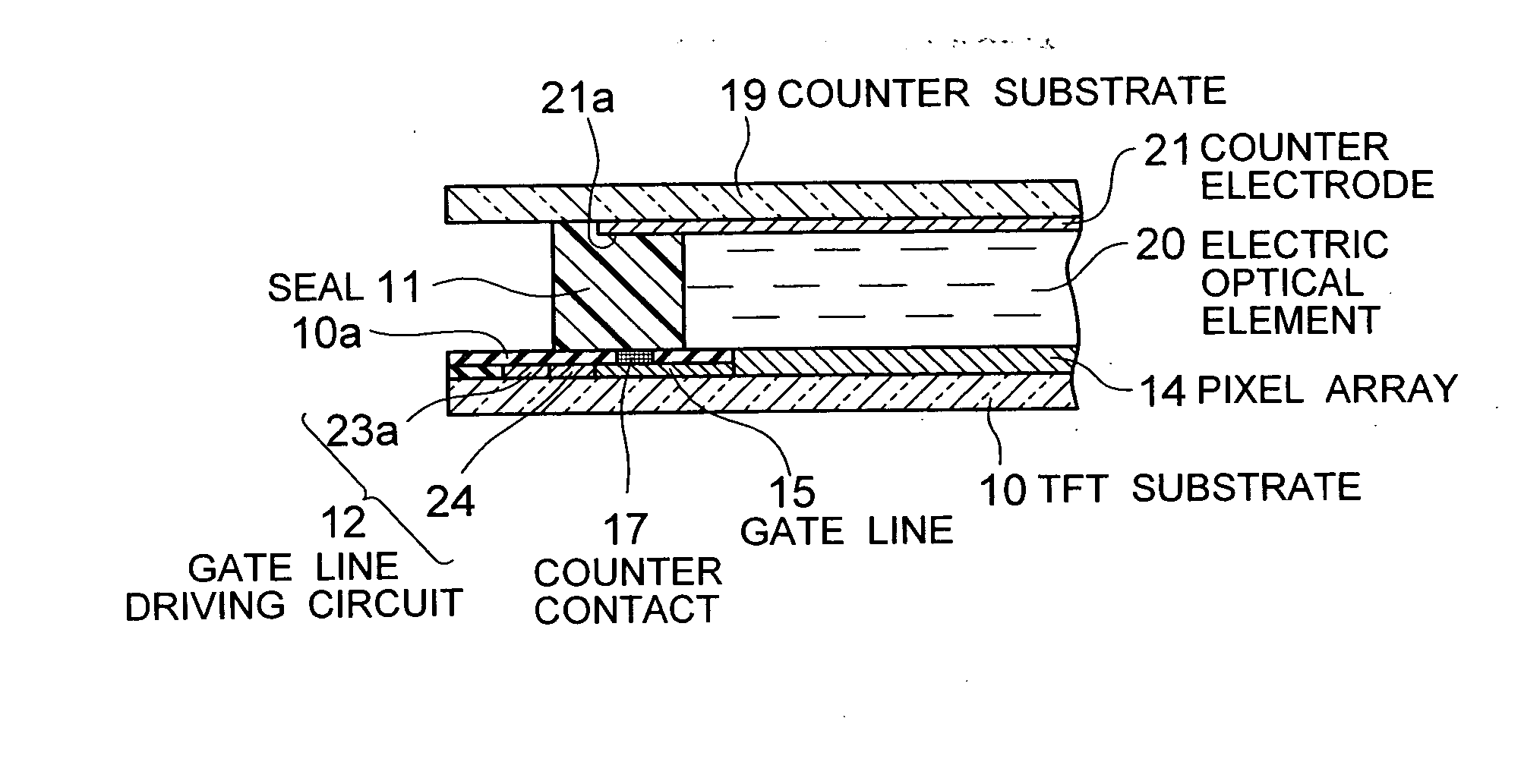
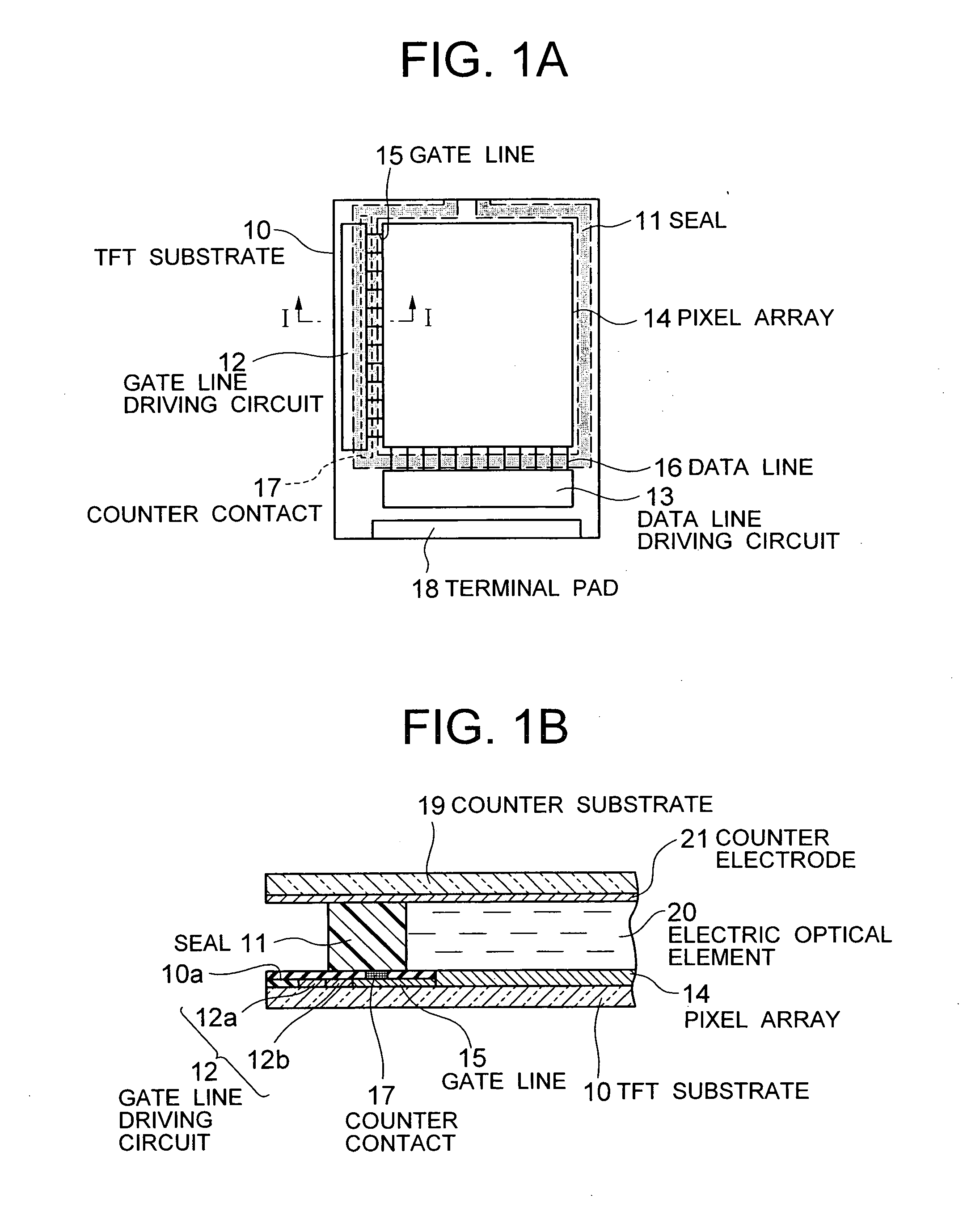
[0080] As shown in FIGS. 1A and 1B, in a display device according to an embodiment 1 of the present invention, a TFT substrate 10 and a counter substrate 19 are disposed opposite each other. A pixel array 14 is formed inside the TFT substrate 10, and a counter electrode 21 is formed inside the counter substrate 19, so that the pixel array 14 of the TFT substrate 10 and the counter electrode 21 of the counter substrate 19 face each other. In a position outside the pixel array 14, a gap in the periphery between the TFT substrate 10 and the counter substrate 19 is sealed with a frame-shaped seal 11. As shown in FIG. 1B, an end part of the TFT substrate 10 is protruded outward from the seal 11 so as to form a gate line driving circuit 12 described later, and corresponding to the dimension of the protruded end part of the TFT substrate 10, an end part of the counter substrate 19 is protruded outward from the seal 11 similarly.

[0081] On the TFT substrate 10, a data line driving circuit 1...

embodiment 2

[0119] In the embodiment 1 shown in FIGS. 3 to 5, NMOS TFT are used as the thin film transistors N1 to N6 constituting the transfer circuit 23 of the gate line driving circuit 12. However, the present invention is not limited to this configuration. A PMOS TFT may be used as the thin film transistor. A case of using a PMOS TFT will be explained as an embodiment 2.

[0120] A display device according to the embodiment 2 has the same configuration as that shown in FIGS. 1A and 1B except that PMOS TFT are used as thin film transistors constituting the transfer circuit 23 of the gate line driving circuit 12. Further, in the embodiment 2, the configuration of the gate line driving circuit 12 is same as that shown in FIG. 2, except that PMOS TFT are used as thin film transistors P1 to P6 as shown in FIG. 7, which is different from the embodiment 1.

[0121] The display device of the embodiment 2 is different from the embodiment 1 in that PMOS TFT are used as thin film transistors P1 to P6 of t...

embodiment 3

[0143] In the embodiments 1 and 2, the gate line driving circuit 12 consists of thin film transistors. However, the present invention is not limited to this configuration. An example in which the circuit element 12a affected by the stray capacitance, in the gate line driving circuit 12, consists of a floating gate of a clocked inverter will be explained as an embodiment 3.

[0144] As shown in FIGS. 11 and 12, in a display device according to the embodiment 3, the gate line driving circuit 12 consists of the transfer circuit 23 corresponding to the circuit element 12a and an output circuit 24 corresponding to the circuit element 12b.

[0145] More specifically, as shown in FIG. 11A, the transfer circuit 23a corresponding to the circuit element 12a consists of a floating gate of a clocked inverter, that is, a combination of the inverter circuit INV1, clocked inverter circuits CINV1 and CINV2 and NAND. As shown in FIG. 11B, the inverter circuit INV1 may have a circuit configuration in whi...


PUM


Abstract

A display device includes: a pair of substrates disposed opposite each other; a conductive seal for sealing the gap of the outer peripheral part between the pair of substrates; an electric optical element disposed in an area defined by the substrates and the seal; a display area, formed on one substrate, having a plurality of pixels for controlling the electric optical element; and a driver circuit for controlling the pixels. The driver circuit is so configured that a circuit element affected by stray capacitance formed between the conductive seal and the driver circuit is disposed apart from the conductive seal.

Description

BACKGROUND OF THE INVENTION [0001] 1. Field of the Invention [0002] The present invention relates to a display device such as an active matrix type one. [0003] 2. Description of Related Art [0004] A conventional driving circuit integrated-type active matrix liquid crystal display will be explained. [0005] As a polysilicon TFT (thin film transistor) formed on an insulating substrate, an expensive quartz substrate was required for a high temperature process, so it was applied to a small display panel with high-value added. Then, a technique for forming a precursor film by low pressure (LP) CVD (chemical vapor deposition), plasma (P) CVD, or sputtering, which is annealed with a laser to thereby polycrystallize, that is, a technique for forming a polysilicon TFT at a low temperature capable of using a glass substrate or the like has been developed. At the same time, an oxide film forming technique, a fine processing technique, a circuit design technique and the like have been developed....

Claims


Application Information

Patent Timeline
IPC IPC(8): G02F1/1345G02F1/1339
CPCG02F1/1339G02F1/13454G02F2001/13606G02F1/13606
Inventor OTOSE, TOMOHIKOSHIGEMURA, KOJI
Owner NEC LCD TECH CORP
Why Eureka
Try Eureka