Exposure apparatus and exposing method and method of manufacturing a printed wiring board

a technology of exposing apparatus and printed wiring board, which is applied in the direction of printers, instruments, data switching networks, etc., can solve the problems of high-output expensive laser sources, inefficient photosensitive reactions, and low photon energy and quantum yield, and achieve low cost, high throughput, and stabilization

Active Publication Date: 2006-09-28
ADTEC ENG
View PDF10 Cites 19 Cited by
  • Summary
  • Abstract
  • Description
  • Claims
  • Application Information

AI Technical Summary

Benefits of technology

[0030] As described above, according to the present invention, it is possible to provide the mask-less direct exposure apparatus which is capable of realizing all requirements for low cost, high throughput, and stabilization of the manufacturing processes, the exposing method for use in the exposure apparatus, and the method of manufacturing a printed wiring board by utilizing the exposing method.

Problems solved by technology

In addition, since both photon energy and quantum yield for electron transition of an infrared radiation are low, the photosensitive reaction does not efficiently occur.
In addition, it is inevitable to use a special photosensitive material containing an infrared absorbing coloring matter and use a high-output expensive laser source.
As a result, it is impossible to sufficiently meet the purposes of realizing a high-quality exposure.
On the other hand, the DMD devices used in JP-A 62-21220, JP-A 2004-157219, and JP-A 2004-39871 do not have sufficient ultraviolet radiation durability.
Thus, in this case as well, a light application period of time required for the photosensitive material to reach desired curing degree becomes long.
Hence, the techniques disclosed in JP-A 62-21220, JP-A 2004-157219, and JP-A 2004-39871 do not meet the purpose of realizing short-time exposure and low cost.
As a result, it is being difficult to respond the requirement for fast production which has been increased more and more recently.
However, even when the intensity of the light source is doubled, the reaction speed is not doubled due to the phenomenon called reciprocity law failure to the exposure and photosensitive reaction.
Hence, it is not always easy to obtain an increase in throughput corresponding to an increase in light source cost.

Method used


Image

  • Exposure apparatus and exposing method and method of manufacturing a printed wiring board
  • Exposure apparatus and exposing method and method of manufacturing a printed wiring board
  • Exposure apparatus and exposing method and method of manufacturing a printed wiring board

Examples


first embodiment

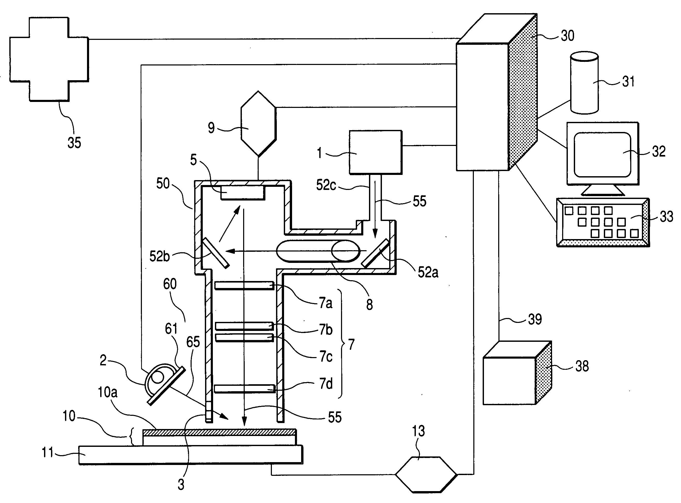
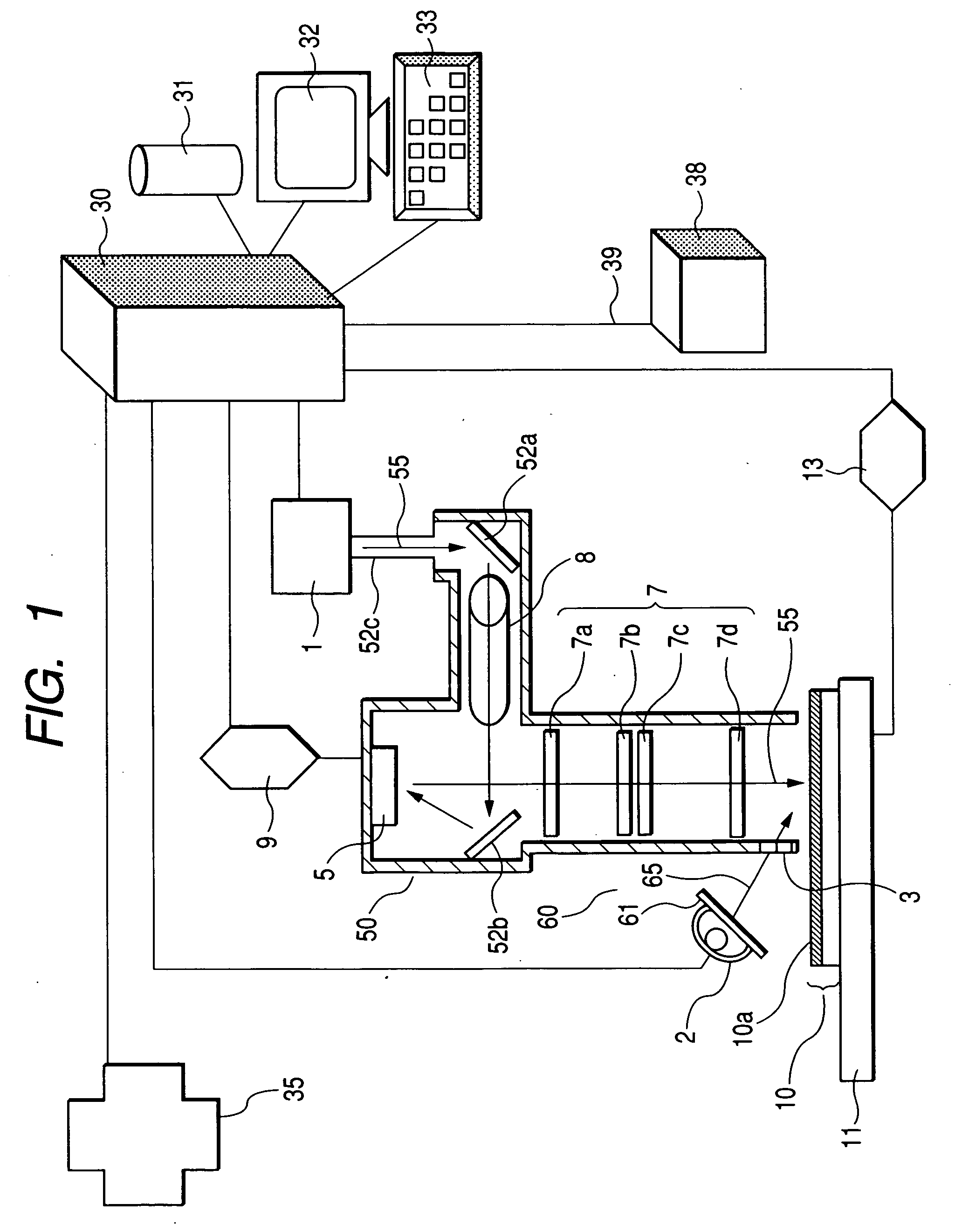
[0042]FIG. 1 is a schematic constructional diagram showing a mask-less exposure apparatus according to the present invention. The mask-less exposure apparatus includes a stage 11, a first light source 1, a first light irradiation optical system 50, a second light source 2, and a second light irradiation optical system 60. The stage 11 moves with a board 10 to be exposed placed thereon. The board 10 has a photosensitive resin layer 10a with sensitivity to ultraviolet radiation formed thereon. The first light source 1 emits light containing a wavelength component, of violet radiation, in the wavelength range of 400 to 410 nm. The first light irradiation optical system 50 modulates a radiant flux 55 emitted from the first light source 1 based on data on a desired exposure pattern, and then images a pattern on the photosensitive resin layer 10a of the board 10 to be exposed which is placed on the stage 11 to expose and write the pattern. The second light source 2 emits light containing ...

second embodiment

[0077]FIG. 9 is a schematic constructional diagram showing the mask-less exposure apparatus according to the present invention. The mask-less exposure apparatus of this embodiment includes a stage 11, a first light source 1, a first light irradiation optical system 50, a second light source 2, and a second light irradiation optical system 60. The stage 11 moves with a board 10 to be exposed placed thereon. The board 10 has a photosensitive resin layer 10a with sensitivity to ultraviolet radiation formed thereon. The first light source 1 emits light containing a wavelength component, of the ultraviolet radiation, in the wavelength range of 350 to 390 nm. The first light irradiation system 50 images a pattern on the photosensitive resin layer 10a on the board 10 to be exposed which is placed on the stage 11 to expose and write the pattern while beam-scanning a radiant flux 55 emitted from the first light source 1 based on data on a desired exposure pattern. The second light source 2 e...

third embodiment

[0084]FIG. 10 is a schematic constructional diagram showing a mask-less exposure apparatus according to the present invention. The mask-less exposure apparatus of this embodiment includes a stage 11, a first light source 1, a second light source 2, an optical mixing system 4, and an optical mixing light irradiation optical system 16. The stage 11 moves with a board 10 to be exposed placed thereon. The board 10 has a photosensitive resin layer 10a with sensitivity to ultraviolet radiation formed thereon. The first light source 1 emits light containing a wavelength component, of the violet radiation, in the wavelength range of 400 to 410 nm. The second light source 2 emits light containing at least a part of a wavelength component, from the visible light to the infrared radiation, in the wavelength range of 450 to 2500 nm. The optical mixing system 4 optically mixes a radiant flux 55 emitted from the first light source 1 and a radiant flux 65 emitted from the second light source 2. Al...


PUM


Abstract

The mask-less exposure apparatus includes: a stage which moves with the substrate having a photosensitive resin layer with sensitivity to ultraviolet radiation formed thereon; a first light source for emitting light containing a wavelength component in the wavelength range of 300 to 410 nm; a first light irradiation optical system for modulating a radiant flux emitted from the first light source based on data of a desired exposure pattern to image a pattern on the photosensitive resin layer; a second light source for emitting light containing a wavelength component in the wavelength range of 450 to 2500 nm; and a second light irradiation optical system for guiding a radiant flux emitted from the second light source to a second light irradiation area that is set so as to include at least a first light irradiation area.

Description

BACKGROUND OF THE INVENTION [0001] The present invention relates to an exposure apparatus and an exposing method for directly writing (drawing) and exposing a pattern on a photosensitive resin without using any of masks (in a mask-less manner), and a printed wiring board manufacturing method of manufacturing a printed wiring board by utilizing the exposing method. [0002] In recent years, a requirement for low cost and / or high throughput production has been increased as multi-item and small-lot production of printed wiring boards has advanced. [0003] In processing a pattern for a printed wiring board or the like in the prior art, various kinds of photosensitive resins called photo resists are used in various processes. More specifically, after a photosensitive liquid resist or dry film resist is coated on a board, the photosensitive liquid resist or dry film resist thus coated is exposed through a photo mask, and etching process, plating process and the like are performed after a dev...

Claims


Application Information

Patent Timeline
Patent Type & Authority Applications(United States)
IPC IPC(8): G03B27/72
CPCG03F7/203G03F7/7005G03F7/70291G03F7/70383G03F7/70466H05K3/0082H04L12/4641H04L63/0272H04L63/0428H04L63/1408
Inventor YAMAGUCHI, YOSHIHIDEOYAMA, HIROSHI
Owner ADTEC ENG
Why Eureka
Try Eureka