

Double-sided wiring board fabrication method, double-sided wiring board, and base material therefor
a fabrication method and wiring board technology, applied in the direction of conductive pattern formation, printed element electric connection formation, chemistry apparatus and processes, etc., can solve the problem of difficulty in fine wiring formation, and achieve the effect of preventing the increase of the total thickness of the conductive film
- Summary
- Abstract
- Description
- Claims
- Application Information
AI Technical Summary
Benefits of technology
Problems solved by technology
Method used
Image

Examples
embodiment 1
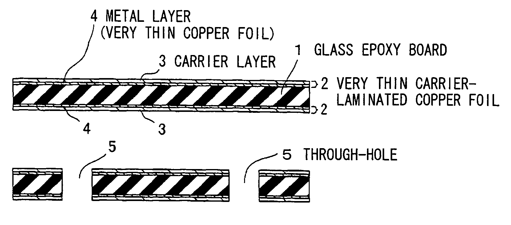
[0073]FIGS. 3A-3G are cross-sectional views showing the respective steps of a double-sided wiring board fabrication process of embodiment 1 according to the invention using a glass epoxy board (through-hole processing).
[0074] A 100 μm thick and 500 mm square glass epoxy board is prepared. The epoxy resin is in a semi-cured state (B-stage state).
[0075] A very thin carrier-laminated copper foil 2“CopperBond® Extra Thin Foil” (Japan Olin Brass Corp.) is bonded to both upper and lower sides of the board 1 using a heat press so as to sandwich the glass epoxy board 1. The copper foil 2 has the sandwich structure comprising very thin copper foil 4 (3 μm) / release layer / carrier copper foil 3 (18 μm). As illustrated in FIG. 3A, the glass epoxy board 1 and the very thin carrier-laminated copper foil 2 are bonded together by laminating the surface of the very thin copper foil 4 on the glass epoxy board 1.
[0076] Using a drill, as illustrated in FIG. 3B, 150 μm-diameter through-holes 5 are for...
embodiment 2
[0082]FIGS. 4A-4I are cross-sectional views showing the respective steps of a double-sided wiring board (flexible double-sided wiring board) fabrication process of embodiment 2 according to the invention using a polyimide board (blind via-hole processing).
[0083] A total 25 μm thick and 70 mm wide polyimide tape (a polyimide board 10) with a thermoplastic polyimide-based adhesive applied to both sides thereof is prepared of a few 10 m.
[0084] Using a heat press, as illustrated in FIG. 4A, a very thin carrier-laminated copper foil 2“CopperBond® Extra Thin Foil” (Japan Olin Brass Corp.) is bonded to one side of the polyimide board 10, and a 12 μm thick electrolytic copper foil 11 is bonded to the other side thereof, so as to sandwich the polyimide board 10. The very thin carrier-laminated copper foil 2 has the sandwich structure comprising very thin copper foil 4 (3 μm) / release layer / carrier copper foil 3 (18 μm). The polyimide board 10 and the very thin carrier-laminated copper foil ...
embodiment 3
[0093]FIGS. 5A-5I are cross-sectional views showing the respective steps of a double-sided wiring board (flexible double-sided wiring board) fabrication process of embodiment 3 according to the invention using a polyimide board (blind via-hole processing).
[0094] A total 25 μm thick and 70 mm wide polyimide tape (a polyimide board 10) with a thermoplastic polyimide-based adhesive applied to both sides thereof is prepared of a few 10 m.
[0095] Using a heat press, as illustrated in FIG. 5A, a very thin carrier-laminated copper foil 2“CopperBond® Extra Thin Foil” (Japan Olin Brass Corp.) is bonded to both sides of the polyimide board 10 so as to sandwich the polyimide board 10. The very thin carrier-laminated copper foil 2 has the sandwich structure comprising very thin copper foil 4 (3 μm) / release layer / carrier copper foil 3 (18 μm). The polyimide board 10 and the very thin carrier-laminated copper foil 2 are bonded together by laminating the surface of the very thin copper foil 4 on ...
PUM
| Property | Measurement | Unit |
|---|---|---|
| thickness | aaaaa | aaaaa |
| thickness | aaaaa | aaaaa |
| thickness | aaaaa | aaaaa |
Abstract
Description
Claims
Application Information