Semiconductor device

a semiconductor and device technology, applied in semiconductor devices, magnetotherapy using permanent magnets, medical science, etc., can solve the problems of difficult to achieve a desired withstand voltage characteristic, difficult to reduce an on-resistance value, and excessive storage of minority carriers (holes) of free carriers. , to achieve the effect of preventing the deterioration of the withstand voltage characteristic, preventing and suppressing the expansion of the depletion layer

Active Publication Date: 2006-10-05
SEMICON COMPONENTS IND LLC
View PDF18 Cites 22 Cited by
  • Summary
  • Abstract
  • Description
  • Claims
  • Application Information

AI Technical Summary

Benefits of technology

[0012] The present invention provides a semiconductor device that includes first and second anode diffusion layers of opposite conductivity types formed on a semiconductor layer of one conductivity type to be isolated therefrom, a cathode diffusion layer of one conductivity type formed on the semiconductor layer, a third anode diffusion layer of an opposite conductivity type formed on the semiconductor layer to be connected to the second anode diffusion layer and extended to the cathode diffusion layer, an insulation layer formed on a top surface of the semiconductor layer, and an anode electrode connected to the first and second anode diffusion layers through a contact hole formed on the insulation layer, and forms a Schottky junction with the semiconductor layer between the first anode diffusion layer and the second anode diffusion layer, wherein at least one of the anode electrode and a metal layer connected to the anode electrode is formed on a top surface of the insulation layer placed at an upper portion of the third anode diffusion layer. Accordingly, in the present invention, since a protection diode is turned on at a forward voltage (Vf) lower than a circuit element, the circuit element can be protected from an overvoltage. Also, in the anode region, the third anode diffusion layer is placed toward the cathode diffusion layer more than the second anode diffusion layer. This structure prevents deterioration in a withstand voltage due to an end portion of the anode electrode, accordingly the protection diode can maintain a desired withstand voltage characteristic.
[0013] Furthermore, in the semiconductor device of the present invention, an end portion of the anode electrode is formed at an upper portion of the second anode diffusion layer of the semiconductor layer. Accordingly, in the present invention, it is possible to reduce a change in a curvature of a depletion layer at a lower portion of the end portion of the anode electrode and to prevent an electric field concentration and deterioration in a withstand voltage characteristic of the protection diode.
[0014] Moreover, in the semiconductor device of the present invention, the second anode diffusion layer is formed of at least two diffusion layers of opposite conductive types each having a different impurity concentration. Accordingly, in the present invention, a diffusion layer having a high impurity concentration can be formed in the vicinity of the end portion of the anode electrode. This structure suppresses an expansion of a depletion layer in an area where the electric field concentration is apt to occur, thereby making it possible to prevent deterioration in a withstand voltage characteristic of the protection diode.

Problems solved by technology

This causes a problem in which a parasitic resistance is high in the epitaxial layer, thereby making it impossible to reduce an ON-resistance value.
As a result, there is a problem in which the electric field concentration is apt to occur in the region where the curvature of the depletion layer is changed, thereby making it difficult to achieve a desired withstand voltage characteristic.
Furthermore, according to the conventional semiconductor device, at a Zener diode operating time, free carriers (holes) which are minority carriers are excessively stored in the N-type epitaxial layer.
Accordingly, there is a problem in which a destruction of a protection diode is caused by the rate of change of the reverse recovery current in time (di / dt).
However, when the above diode is used as a protection diode for a circuit element that forms a high frequency circuit, there is a problem in which a parasitic capacitance of the Zener diode is increased to cause deterioration in a high frequency characteristic.

Method used


Image

  • Semiconductor device
  • Semiconductor device
  • Semiconductor device

Examples


Embodiment Construction

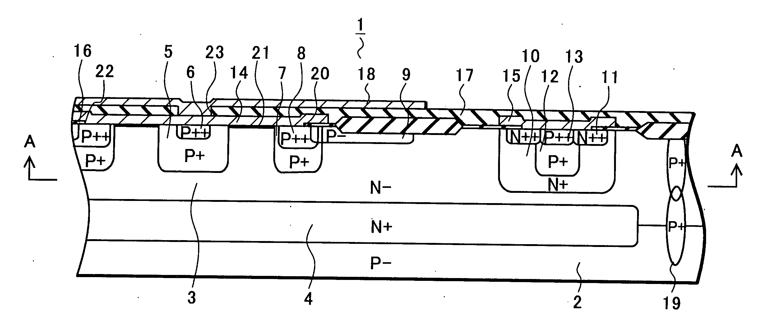
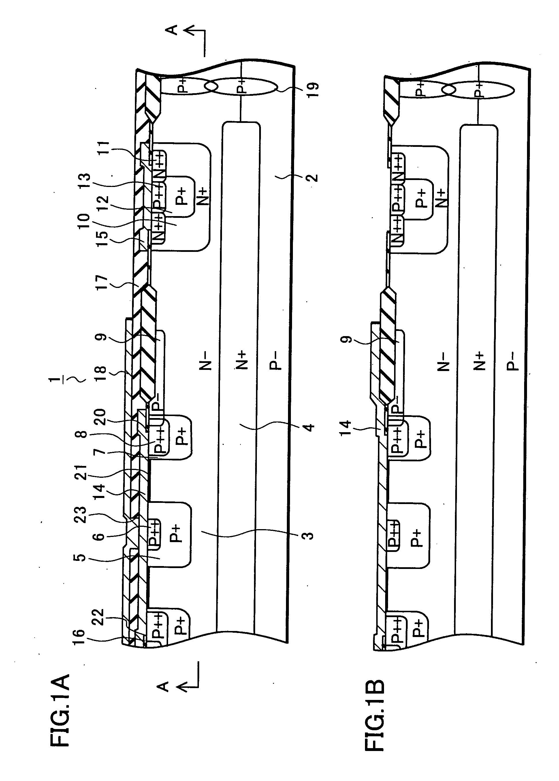
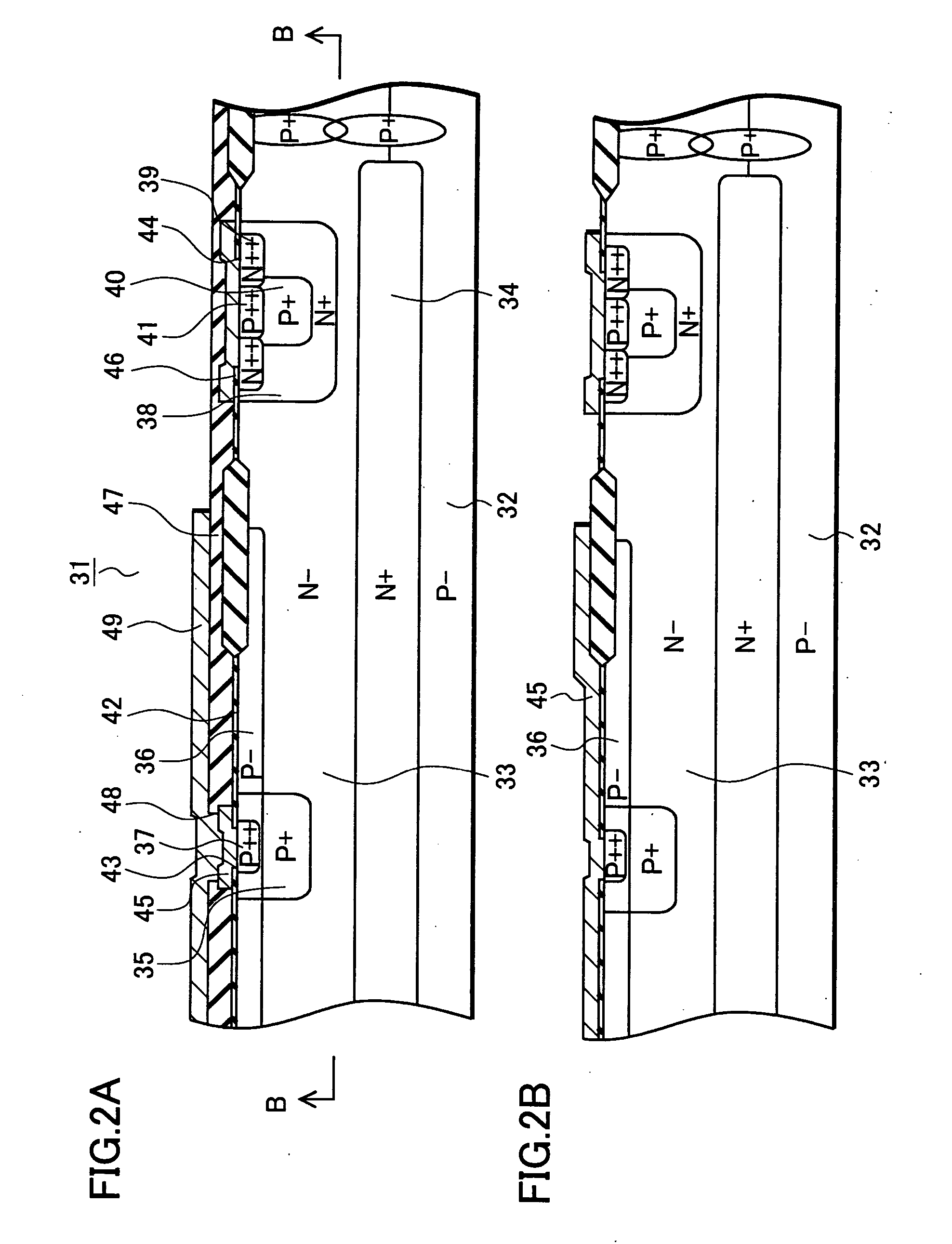
[0028] The following will specifically explain a semiconductor device according to one embodiment of the present invention with reference to FIGS. 1 to 7. FIG. 1A and FIG. 1B are cross-sectional views each explaining a protection diode according to one embodiment of the present invention. FIG. 2A and FIG. 2B are cross-sectional views each explaining a Zener diode according to the embodiment. FIG. 3 is a view explaining a forward voltage (Vf) of each of the protection diode and a Zener diode according to the embodiment. FIG. 4 is a view explaining a circuit into which the protection diode is incorporated according to the embodiment. FIG. 5A is a view explaining an electric potential distribution of the protection diode in a reverse bias state according to the embodiment. FIG. 5B is a view explaining an impact ionization occurring region in the protection diode according to the embodiment. FIG. 6 is a view explaining an electric potential distribution of the protection diode in a reve...


PUM


Abstract

In a semiconductor device of the present invention, a protection diode for protecting a device is formed on an epitaxial layer formed on a substrate. A Schottky barrier metal layer is formed on a surface of the epitaxial layer and a P-type diffusion layer is formed at a lower portion of an end portion of the Schottky barrier metal layer. Then, a P-type diffusion layer is formed to be connected to a P-type diffusion layer and is extended to a cathode region. A metal layer to which an anode electrode is applied is formed above the P-type diffusion layer, thereby making it possible to obtain a field plate effect. This structure reduces a large change in a curvature of a depletion layer, thereby improving a withstand voltage characteristic of the protection diode.

Description

[0001] Priority is claimed to Japanese Patent Application Numbers JP2005-098965, filed on Mar. 30, 2005, and JP2006-064619, filed on Mar. 9, 2006, the disclosures of which are incorporated herein by reference in its entireties. BACKGROUND OF THE INVENTION [0002] 1. Field of the Invention [0003] The present invention relates to a semiconductor device that protects a circuit element from an overvoltage. [0004] 2. Description of the Related Art [0005] In a conventional semiconductor device, an N-type epitaxial layer is formed on an N-type semiconductor substrate. A P-type diffusion layer is overlapped onto an N-type diffusion layer formed on the epitaxial layer. Then, an anode electrode is formed on the P-type diffusion layer, and a cathode electrode is formed on a back surface of the substrate to form a Zener diode using a PN junction of both diffusion layers. A P-type guard region is formed around the P-type diffusion layer and another guard region is formed on its outer side. A Scho...

Claims


Application Information

Patent Timeline
Patent Type & Authority Applications(United States)
IPC IPC(8): H01L29/861
CPCH01L29/872H01L29/866A61F5/0102A61F5/028A61F13/148A61N2/06
Inventor KIKUCHI, SHUICHIOKAWA, SHIGEAKINAKAYA, KIYOFUMITAKAHASHI, TOSHIYUKI
Owner SEMICON COMPONENTS IND LLC
Why Eureka
Try Eureka