Semiconductor wafer having multiple semiconductor elements and method for dicing the same

a technology of semiconductor elements and semiconductor wafers, applied in the field of semiconductor wafers, can solve the problems of increasing the manufacturing cost of each chip, difficult to form the modified region on the multi-layer wafer, and difficult to form the modified region uniformly, so as to achieve high yield ratio and high quality

Inactive Publication Date: 2006-10-05
DENSO CORP
View PDF7 Cites 30 Cited by
  • Summary
  • Abstract
  • Description
  • Claims
  • Application Information

AI Technical Summary

Benefits of technology

[0009] In view of the above-described problem, it is an object of the present invention to provide a semiconductor wafer having multiple semiconductor elements with high yielding ratio and high quality. It is another object of the present invention to provide a method for dicing a semiconductor wafer having multiple semiconductor elements.
[0011] In the above wafer, the laser beam is irradiated on the first layer without passing through the second layer. Specifically, in the layer removal region, no second layer exists. Here, the second layer causes reflection and / or scattering of the laser beam when the laser beam is entered into the first layer from the second layer side. Thus, the laser beam is irradiated on the first layer without reflection and scattering so that the modified region is formed at a preliminarily designed region in the first layer. Accordingly, the wafer can be separated, i.e., deiced with accuracy. Specifically, each semiconductor element can be separated with high yielding ratio and high quality.
[0013] In the above method, the laser beam is irradiated on the first layer without passing through the second layer. Specifically, in the layer removal region, no second layer exists. Here, the second layer causes reflection and / or scattering of the laser beam when the laser beam is entered into the first layer from the second layer side. Thus, the laser beam is irradiated on the first layer without reflection and scattering so that the modified region is formed at a preliminarily designed region in the first layer. Accordingly, the wafer can be separated, i.e., deiced with accuracy. Specifically, each semiconductor element can be separated with high yielding ratio and high quality.
[0015] In the above wafer, the laser beam is irradiated on the first layer without passing through the top layer. Specifically, in the layer removal region, no top layer exists. Here, the top layer causes reflection and / or scattering of the laser beam when the laser beam is entered into the first layer from the second layer side. Thus, the laser beam is irradiated on the first layer without reflection and scattering so that the modified region is formed at a preliminarily designed region in the first layer. Accordingly, the wafer can be separated, i.e., deiced with accuracy. Specifically, each semiconductor element can be separated with high yielding ratio and high quality.

Problems solved by technology

A manufacturing cost of each chip increases.
However, it is difficult to form the modified region on the multi-layer wafer.
In a case of the multi-layer wafer, it is difficult to form the modified region uniformly.
By using the multiple photon absorption effect, optical damage is generated on the material at a focal point and around the focal point.
The optical damage induces thermal distortion.
Thus, a crack is generated at a portion, at which the thermal distortion is occurred.

Method used


Image

  • Semiconductor wafer having multiple semiconductor elements and method for dicing the same
  • Semiconductor wafer having multiple semiconductor elements and method for dicing the same
  • Semiconductor wafer having multiple semiconductor elements and method for dicing the same

Examples


first embodiment

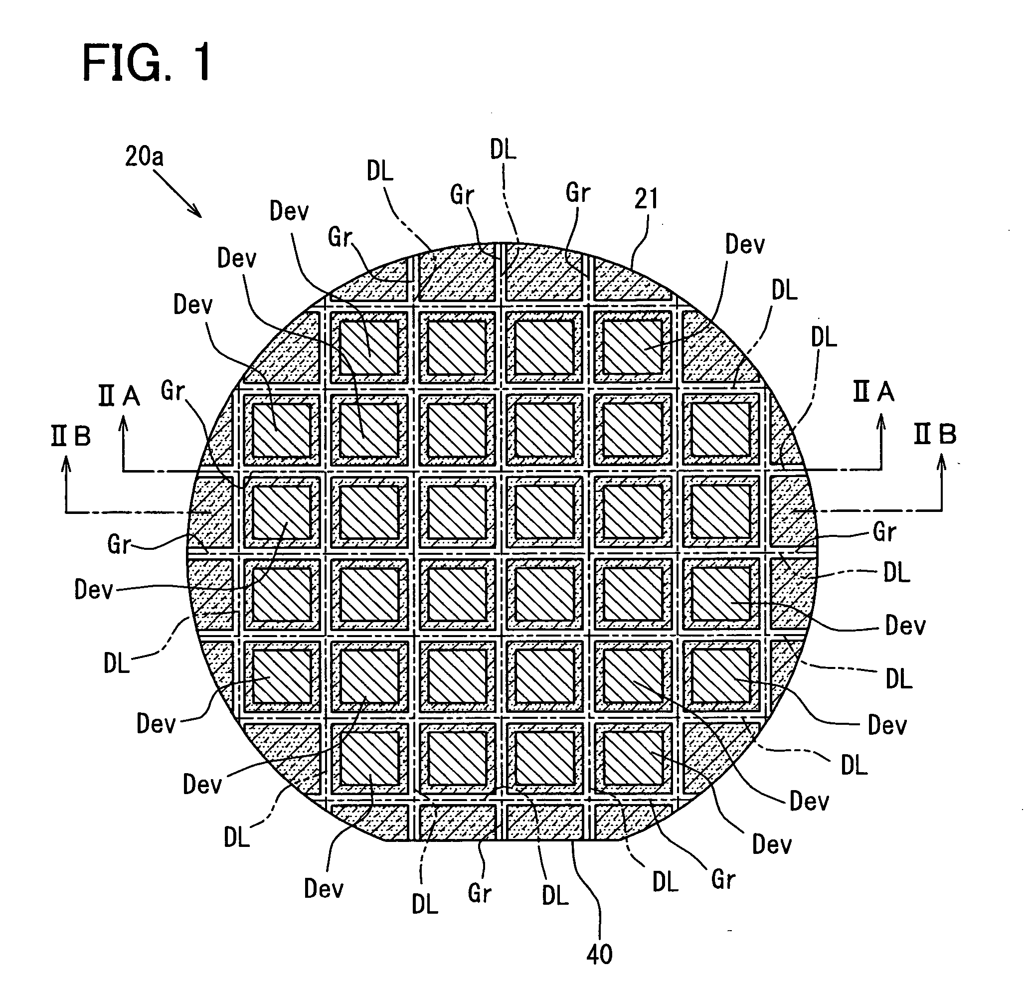
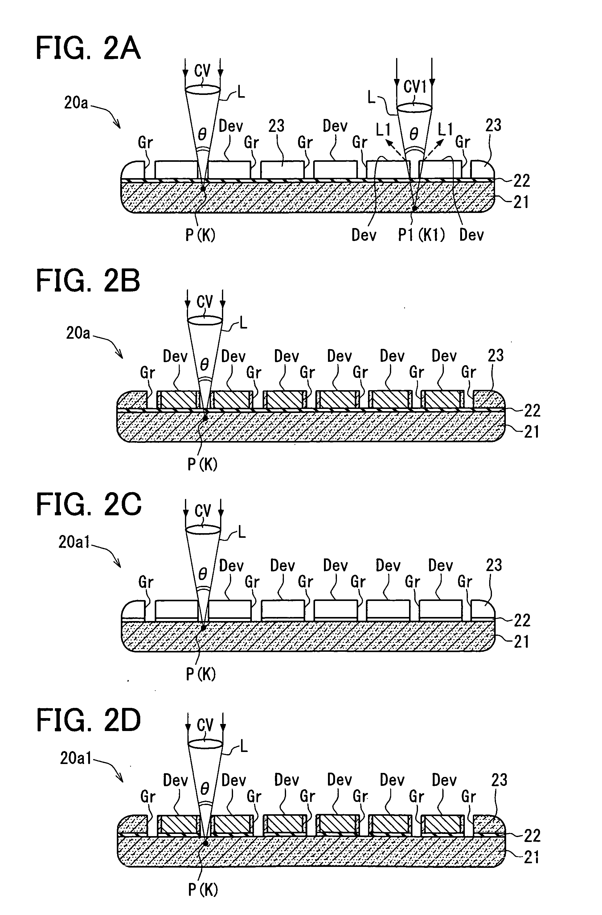
[0027] A semiconductor wafer 20a according to a first embodiment of the present invention is shown in FIG. 1. The wafer 20a is a silicon substrate 21 having a thin disk shape and made of silicon. The wafer 20a includes an orientation flat 40 for representing a crystal orientation. The orientation flat 40 of the wafer 20a is disposed on a part of an outer periphery of the wafer 20a. As shown in FIGS. 2A and 2B, the wafer 20a includes a silicon substrate 21, an embedded oxide layer 22 and a SOI layer 23, which are stacked in this order. Thus, the wafer 20a is a SOI wafer having multi-layer structure.

[0028] On the surface of the wafer 20a, multiple chips Dev are arranged to be a grid. Each chip Dev is formed on the wafer 20a in a semiconductor process such as a diffusion step. The wafer 20a is separated into the chips Dev by using a laser beam. The laser beam is scanned along with a cutting line DL, i.e., a dicing line.

[0029] A layer removal region as a groove Gr is formed on the waf...

second embodiment

[0041] A semiconductor wafer 20b according to a second embodiment of the present invention is shown in FIGS. 4, 5A and 5B. In the wafer 20b, the layer removal region, i.e., the groove Gr, is formed around the chip Dev. Therefore, the groove Gr does not reach the outer periphery of the wafer 20b. The groove Gr in the wafer 20b is not formed in an outer periphery region R, so that the groove does not disposed from one outer periphery end of the wafer 20b to the other outer periphery end.

[0042] As shown in FIG. 4, the groove Gr along with the cutting line DL is formed in such a manner that the groove Gr surrounds multiple chips Dev in the wafer 20b. Specifically, the groove Gr surrounds a chip to be formed region. Thus, the groove Gr in the wafer 20b is formed to minimize an area of the groove Gr on the cutting line DL of the laser beam L. The groove Gr is formed in a necessity minimum area for separating all chips Dev. In the groove Gr, only part of the SOI layer 23 is removed from t...

third embodiment

[0045] A semiconductor wafer 20c according to a third embodiment of the present invention is shown in FIGS. 6, 7A and 7B. In the wafer 20c, an outer layer removal region Gr1 disposed in the outer periphery region R is formed. Specifically, the outer layer removal region Gr1 is disposed on an outside from the utmost outer chip Dev1. Here, the outer periphery region R is disposed outside of the utmost outer chip Dev1, which is disposed on the utmost outside of the wafer 20c. The outer layer removal region Gr1 is formed on a wide area including the cutting line DL. Thus, not only the groove Gr as the layer removal region but also the outer layer removal region Gr1 are formed in the wafer 20c so that the groove Gr and the outer layer removal region Gr1 are disposed on the wafer 20c other than the chips Dev and its surrounding area. Here, in the wafer 20c, only a part of the SOI layer 23 is removed from the wafer 20c, and the oxide layer 22 and the silicon substrate 21 are not removed fr...


PUM


Abstract

A semiconductor wafer includes: a first layer having a first refraction index; a second layer having a second refraction index, which is different from the first refraction index; a plurality of semiconductor elements; and a layer removal region. The semiconductor elements are capable of being separated each other by irradiating a laser beam on the first layer along with a cutting line. The laser beam irradiation provides a modified region in the first layer so that the semiconductor elements are capable of being separated by a crack generated in the modified region. The layer removal region is provided such that the second layer in the layer removal region is removed from the wafer.

Description

CROSS-REFERENCE TO RELATED APPLICATION [0001] This application is based on Japanese Patent Application No. 2005-101554 filed on Mar. 31, 2005, the disclosure of which is incorporated herein by reference. FIELD OF THE INVENTION [0002] The present invention relates to a semiconductor wafer having multiple semiconductor elements and a method for dicing the same. BACKGROUND OF THE INVENTION [0003] As shown in FIGS. 8A to 8C, a silicon wafer 100 includes a semiconductor integrated circuit or MEMS (i.e., micro electro mechanical systems) as a semiconductor element. Specifically, the wafer 100 includes multiple chips Dev. In a step of separating the wafer into each chip Dev, i.e., in a dicing step, the wafer 100 is cut by a dicing blade along with a cutting line DL so that the wafer is divided into multiple chips Dev. The dicing blade has a diamond abrasive grain embedded in the blade. [0004] When the dicing blade is used in the dicing step, a cutting width is necessitated. Therefore, the ...

Claims


Application Information

Patent Timeline
Patent Type & Authority Applications(United States)
IPC IPC(8): H01L29/06H01L21/00
CPCH01L21/78H01L21/67132
Inventor ASAI, MAKOTOTAMURA, MUNEOSUGIURA, KAZUHIKOFUJII, TETSUO
Owner DENSO CORP
Why Eureka
Try Eureka