

Piezoelectric film laminate and method of manufacturing the same
a technology of film laminate and piezoelectric film, which is applied in the direction of zirconium compounds, natural mineral layered products, coatings, etc., can solve the problems of high electromechanical coupling factor, high sound speed, and inability to achieve zero temperature properties
- Summary
- Abstract
- Description
- Claims
- Application Information
AI Technical Summary
Problems solved by technology
Method used
Image

Examples
first embodiment
1. First Embodiment
[0068] 1.1 Piezoelectric Film Laminate
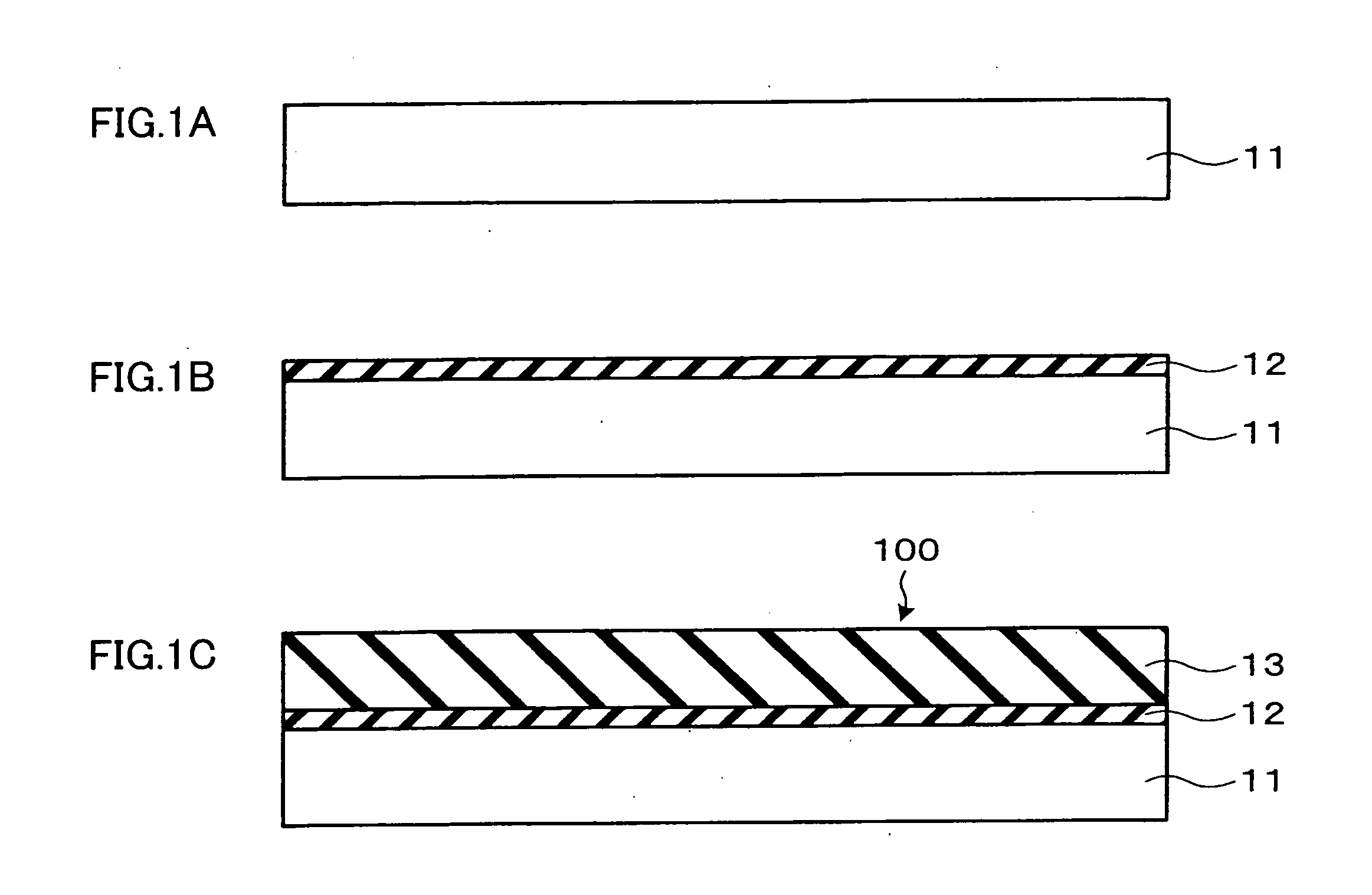
[0069]FIG. 1C is a cross-sectional view schematically showing a piezoelectric film laminate 100 according to a first embodiment.
[0070] As shown in FIG. 1C, the piezoelectric film laminate 100 according to the first embodiment may include a substrate 11 and a piezoelectric film laminate formed on the substrate 11 and including a lead zirconate titanate niobate film 12 and a potassium niobate film 13.
[0071] As the substrate 11, an R-plane sapphire substrate may be used. It is preferable to use the R-plane sapphire substrate because the R-plane sapphire substrate allows the lead zirconate titanate niobate film 12 to be epitaxially grown, is inexpensively available as a large substrate, and can be repeatedly used due to etchant resistance.
[0072] The lead zirconate titanate niobate (Pb(Zn,Ti,Nb)O3) (hereinafter may be called “PZTN”) film 12 is epitaxially grown in a tetragonal (110) or (101) orientation or a rhombohedral (110) ...
example 1
1.3 EXAMPLE 1
[0144] In Example 1, the piezoelectric film laminate 100 (see FIG. 1C) was formed by the following method. In Example 1, a single crystal lead zirconate titanate niobate thin film and a single crystal potassium niobate thin film were obtained.
[0145] The R-plane sapphire substrate 11 made of an R surface sapphire single crystal substrate was immersed in an organic solvent and cleaned by washing using an ultrasonic washing machine. As the organic solvent, a 1:1 mixed solution of ethyl alcohol and acetone was used.
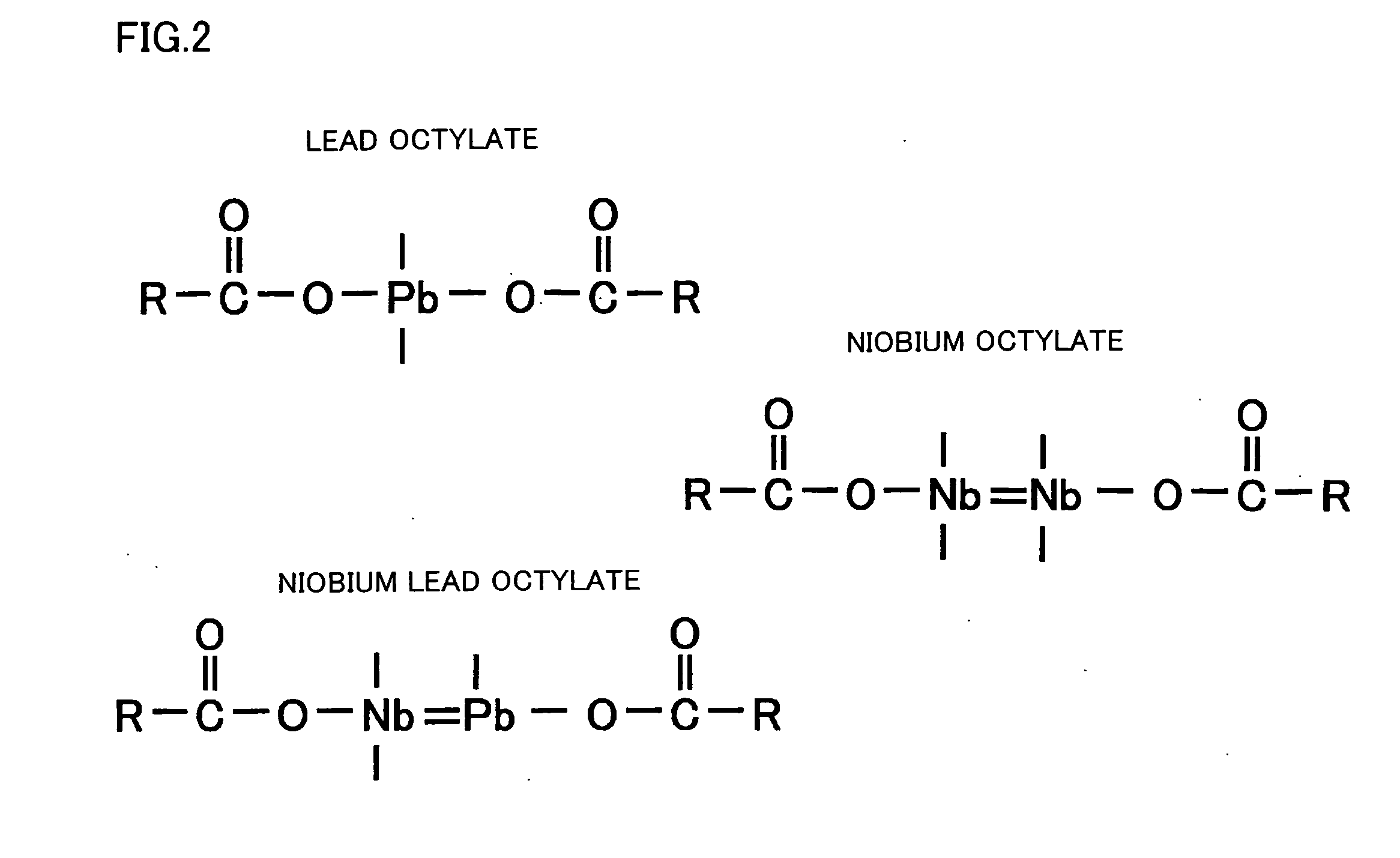
[0146] In Example 1, a precursor composition was obtained as follows. Specifically, the precursor composition was obtained by mixing first to third raw material solutions, each containing at least one of Pb, Zr, Ti, and Nb, dimethyl succinate as the polycarboxylic acid ester, and n-butanol as the organic solvent. The mixed solution was prepared by dissolving the sol-gel raw material and dimethyl succinate in n-butanol at a ratio of 1:1 (molar ionic concentratio...
second embodiment
2. Second Embodiment
[0158] 2.1. Piezoelectric Film Laminate
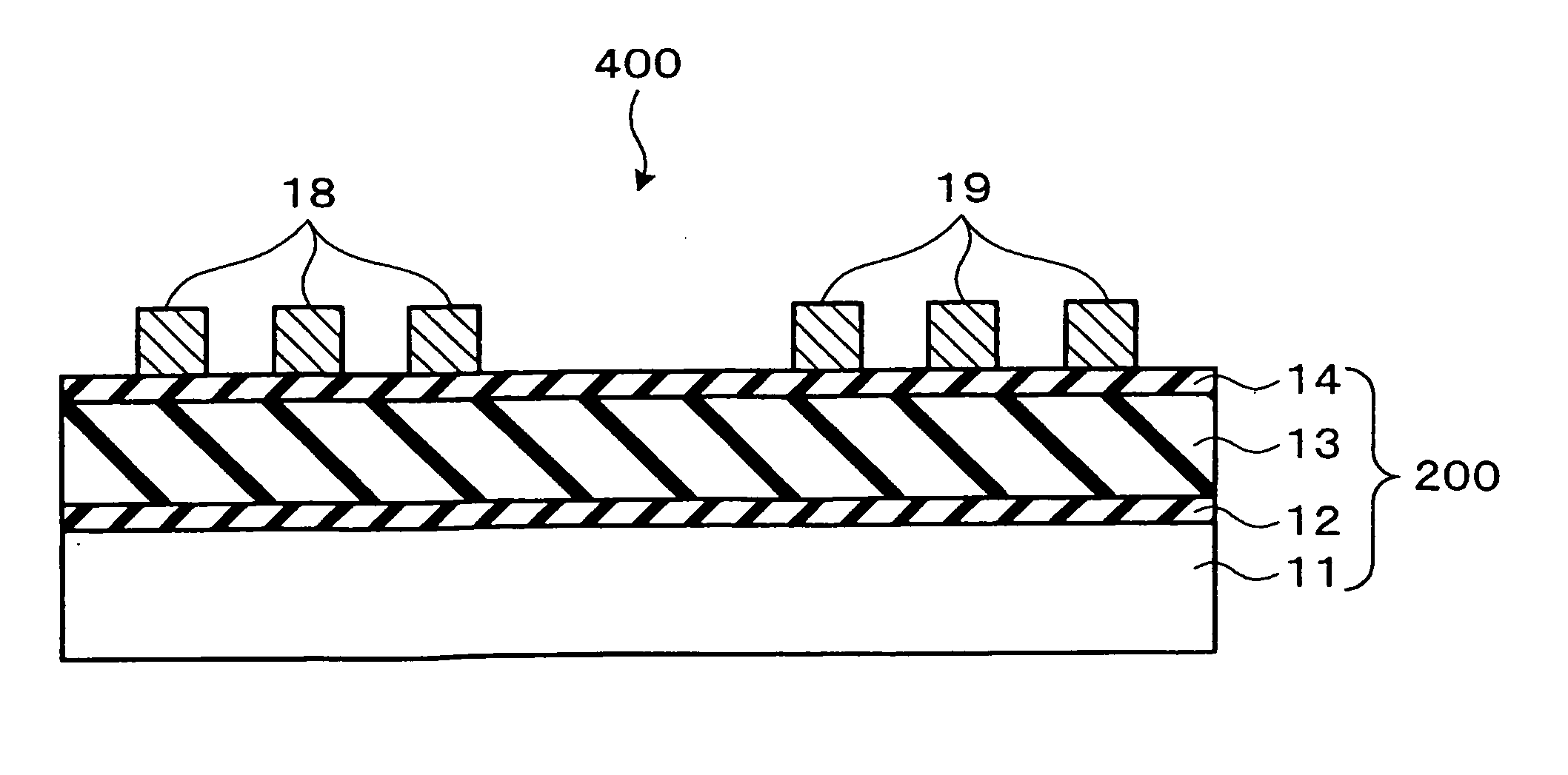
[0159]FIG. 8 is a cross-sectional view schematically showing a piezoelectric film laminate 200 according to a second embodiment.
[0160] As shown in FIG. 8, the piezoelectric film laminate 200 according to the second embodiment may include the substrate 11, and a piezoelectric film laminate formed on the substrate 11 and including the first lead zirconate titanate niobate film 12, the potassium niobate film 13, and a second lead zirconate titanate niobate film 14. The substrate 11, the first lead zirconate titanate niobate film 12, and the potassium niobate film 13 are substantially the same as those of the piezoelectric film laminate 100 according to the first embodiment. The second embodiment merely differs from the first embodiment in that the second lead zirconate titanate niobate film 14 is formed on the potassium niobate film 13. Therefore, detailed description of the same members as in the first embodiment is omitted....
PUM
| Property | Measurement | Unit |
|---|---|---|
| crystallization temperature | aaaaa | aaaaa |
| thickness | aaaaa | aaaaa |
| thickness | aaaaa | aaaaa |
Abstract
Description
Claims
Application Information