Semiconductor device

a technology of semiconductor elements and diodes, applied in the field of diodes, can solve the problems that the mos transistor b>20/b>-b>1/b> cannot serve as a semiconductor element, and achieve the effect of preventing the gate insulating film from being damaged and reducing the current flowing

Inactive Publication Date: 2006-10-12
LAPIS SEMICON CO LTD
View PDF3 Cites 37 Cited by
  • Summary
  • Abstract
  • Description
  • Claims
  • Application Information

AI Technical Summary

Benefits of technology

[0023] Further, in the semiconductor device according to the second aspect of the invention, since the dummy conductive pattern is provided, it is possible to reduce a current flowing fr

Problems solved by technology

As a result, the MOS transistor 20-1 c

Method used


Image

  • Semiconductor device
  • Semiconductor device
  • Semiconductor device

Examples


first embodiment

[0048] (Configuration of First Embodiment)

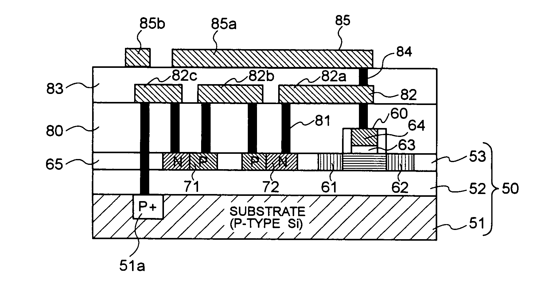
[0049] FIGS. 7 to 10 are views schematically illustrating the configuration of a semiconductor device using an SOI substrate according to a first embodiment of the invention. Specifically, FIG. 7 is a longitudinal sectional view illustrating the configuration of the semiconductor device, FIG. 8 is a top plan view illustrating the configuration of the semiconductor device, FIG. 9 is a circuit diagram of the semiconductor device, and FIG. 10 is a wave form chart illustrating an operation of the semiconductor device.

[0050] The semiconductor device according to the first embodiment shown in FIGS. 7 and 8 has, for example, a two-layered wiring structure. In the semiconductor device, a semiconductor element (for example, MOS transistor) 60 and a protection circuit (for example, a series circuit composed of a NP junction diode 72 and an PN junction diode 71) for protecting the semiconductor element 60 are formed on the SOI substrate 50. The SOI su...

fourth embodiment

[0096] In the fourth embodiment, since the dummy conductive patterns 91 to 97 not related to the circuit are provided and the dummy conductive patterns 91 to 97 are connected to the support substrate 51 through the vias 81, 84, and 87, it is possible to reduce a current supplied to the NP junction diode 72 from a bottom surface of the support substrate 51. When n dummy conductive patterns 91, . . . are provided for one NP junction diode, the charges existing on the bottom surface of the support substrate 51 are divided. For example, assuming that the area of the dummy conductive pattern 91, . . . and the wiring area connected to the NP junction diode 72 is k multiples, a current, which flows through the NP junction diode 72 due to the bottom-surface charges of the support substrate 51 during a wiring line etching process, is reduced to k / n+k, and a current, which flows through the NP junction diode 72 due to the charges existing on the bottom surface of the support substrate 51 duri...

fifth embodiment

[0104] Assuming that the total area of the device unit 100 in the respective wiring layers is S1 and a pattern area S2 of an antenna composed of the dummy conductive patterns 101 to 103 in the respective wiring layers is S2, in the same manner as in the fifth embodiment, a current, which flows through the NP junction diode 72 due to the bottom-surface charges of the support substrate 51 during a wiring line etching process, is reduced to S1 / (S1+S2), and a current, which flows through the NP junction diode 72 due to the bottom-surface charges of the support substrate 51 during a via etching process, is reduced to 1 / n+1.

[0105] As such, even when the line-shaped dummy conductive patterns 101 to 103 are used, it is possible to obtain almost the same operation and effects as in the fifth embodiment. In particular, by surrounding the periphery of the device unit 100 with the line-shaped dummy conductive patterns 101 to 103, the distribution of top-surface / bottom-surface charges of the sup...


PUM


Abstract

A semiconductor element is configured to prevent deterioration thereof due to an electrical charge occurring at a top surface/bottom surface of a support substrate during a plasma process in manufacturing a semiconductor device using an SOI substrate. The semiconductor device includes a MOS transistor formed on an SOI layer of the SOI substrate; a wiring pattern which is formed on an interlayer insulating film covering the SOI layer and is connected to a gate electrode or a diffusion layer of the MOS transistor through a via; and a protection circuit which is connected between the support substrate of the SOI substrate and the wiring pattern and which, when the amount of charges generated with respect to the gate electrode during a plasma process of forming the wiring pattern exceeds a predetermined value, discharges the charges toward the support substrate or blocks the charges. For example, the protection circuit includes a series circuit of a PN junction diode and an NP junction diode each having a breakdown voltage value corresponding to the predetermined value.

Description

BACKGROUND OF THE INVENTION [0001] 1. Field of the Invention [0002] The present invention relates to a semiconductor device using an SOI (silicon-on-insulator) substrate, and in particular, to a technique for preventing deterioration of a semiconductor element caused by the electric charge occurring at a top surface / bottom surface of a support substrate during a plasma process in manufacturing the semiconductor device. [0003] 2. Description of the Related Art [0004] A technique for preventing deterioration of a semiconductor element in a process (plasma process) of manufacturing a conventional semiconductor device using an SOI substrate is disclosed in Japanese Patent Kokai No. 2003-133559 (patent document 1), FIG. 2, for example. [0005] FIGS. 1 to 3 are views schematically illustrating the configuration of a conventional semiconductor device using an SOI substrate. Specifically, FIG. 1 is a longitudinal sectional view illustrating the configuration of the semiconductor device and s...

Claims


Application Information

Patent Timeline
IPC IPC(8): H01L27/12
CPCH01L27/1203H01L27/0251A01G9/02E02B3/129E02B3/14E02D17/205
Inventor ARAKAWA, YOSHIKAZU
Owner LAPIS SEMICON CO LTD
Why Eureka
Try Eureka