

Ballistic semiconductor device
a semiconductor device and ballistic technology, applied in the field of ballistic semiconductor devices, can solve the problems of small device gain, low operation speed, and smaller device gain than that of a general transistor, and achieve the effect of half the energy level of permeability coefficient and higher operation speed
- Summary
- Abstract
- Description
- Claims
- Application Information
AI Technical Summary
Benefits of technology
Problems solved by technology
Method used
Image

Examples
first embodiment
[0048] According to a first embodiment of the present invention, there is provided a novel ballistic semiconductor device which is easy to fabricate, and operates at a high speed in a wide temperature range, as compared to the conventional ballistic semiconductor device.
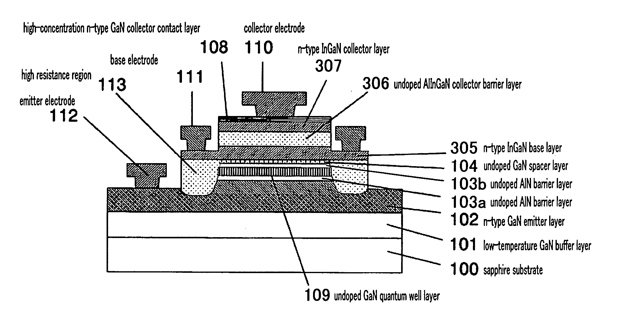
[0049]FIG. 1 is a cross-sectional view showing an example of a cross-sectional structure of the ballistic semiconductor device according to this embodiment. The ballistic semiconductor device according to this embodiment is a RHET. This ballistic semiconductor device comprises a sapphire substrate 100. On the sapphire substrate 100, a low-temperature GaN buffer layer (with a film thickness d=100 nm) 101, a n-type GaN emitter layer (with a carrier concentration n=1018 cm−3, d=1 μm) 102, an undoped AlN barrier layer 103a, an undoped GaN quantum well layer 109, an undoped AlN barrier layer 103b, an undoped GaN spacer layer 104, a n-type InGaN base layer (n=1018 cm−3) 305, an undoped AlInGaN collector barrier layer 306,...
second embodiment
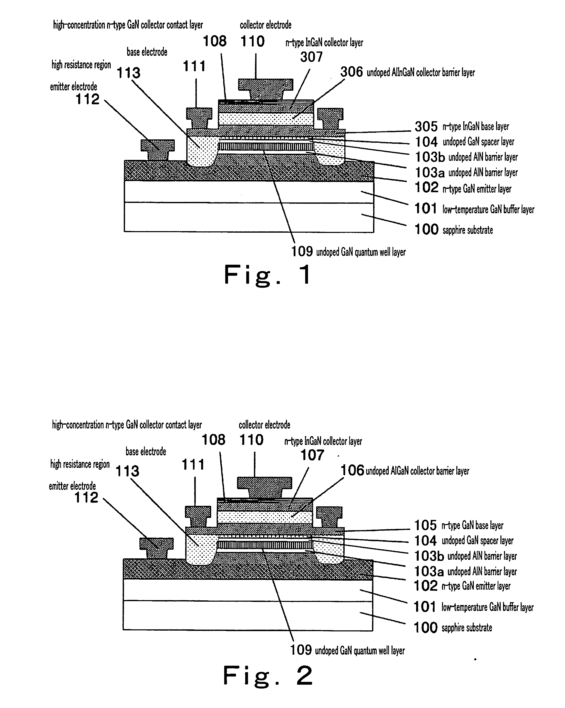
[0088] In a second embodiment of the present invention, the collector layer 107 is first formed on the GaN substrate. In the first embodiment, the barrier layers 103a and 103b and the quantum well layer 109 each forming the resonant-tunneling structure are required to have uniform film thickness and flatness. Therefore, the resonant-tunneling structure is first formed on the GaN substrate. But in order to reduce parasitic capacitance or the like, the emitter is preferably smaller.
[0089] Accordingly, in this embodiment, the collector is first formed on the GaN substrate.
[0090]FIG. 5 is a cross-sectional view showing a cross-sectional structure of a ballistic semiconductor device according to this embodiment. In FIG. 5, the same reference numerals as those in FIG. 1 denote same or corresponding portions.
[0091] As shown in FIG. 5, in the ballistic semiconductor device of this embodiment, the defect reduction layer 201 comprising the AlGaN / GaN super lattice structure, the n-type InGa...
third embodiment
[0100] According to a third embodiment of the present invention, there is provided a novel ballistic semiconductor device capable of achieving amplification ratio larger than that of the first and second embodiments.
[0101]FIG. 6 is a cross-sectional view showing a cross-sectional structure of the ballistic semiconductor device according to this embodiment. In FIG. 6, the same reference numerals as those in FIG. 5 denote same or corresponding portions.
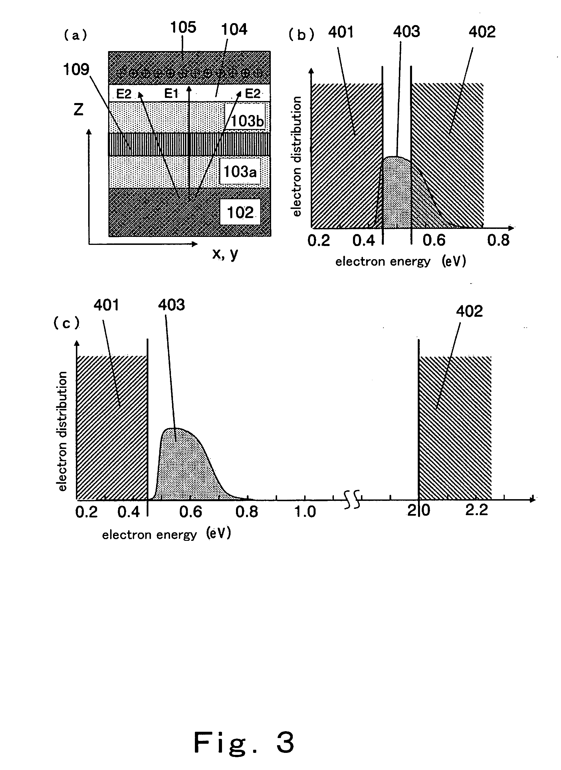
[0102] As shown in FIG. 6, in this embodiment, a quantum well layer 209 is formed by an undoped InGaN layer, unlike in the second embodiment in which the quantum well layer 109 is formed by the undoped GaN layer. Other configuration is identical to that of the second embodiment.
[0103] In the undoped InGaN quantum well layer 209, composition ratio (concentration) of In is not less than 10% and not more than 30%. The InGaN quantum well layer 209 is grown while simultaneously feeding In, Ga, and N. A growth speed is set to 0.1 μm / h, whi...
PUM
 Abstract
Description
Claims
Application Information