Power clamp circuit and semiconductor device

a power clamp circuit and semiconductor technology, applied in the field of semiconductor devices, can solve the problems of increasing current consumption and accelerating the consumption of battery current, and achieve the effect of increasing current consumption

Inactive Publication Date: 2006-10-19
FUJITSU MICROELECTRONICS LTD
View PDF8 Cites 17 Cited by
  • Summary
  • Abstract
  • Description
  • Claims
  • Application Information

AI Technical Summary

Benefits of technology

[0009] However, an H level signal is output from the buffer circuit 55 to the transistor 56 to activate the transistor 56 on, not only when a high voltage surge such as ESD is applied to the power supply terminal 59, but also when power supply noise having a displacement potential that is greater than or equal to the voltage that activates the transistor 61 of the buffer circuit 55 (i.e., the threshold voltage) is applied to the power supply terminal 59. Therefore, even if the power supply noise is at a to...

Problems solved by technology

Such a power supply leak current increases current consumption.
Especially when the LSI 52 configures a ba...

Method used


Image

  • Power clamp circuit and semiconductor device
  • Power clamp circuit and semiconductor device
  • Power clamp circuit and semiconductor device

Examples


first embodiment

[0025] A power clamp circuit 1 according to the present invention will now be described with reference to FIGS. 2 to 5.

[0026]FIG. 2 is a schematic circuit diagram showing the power clamp circuit 1 according to a first embodiment of the present invention.

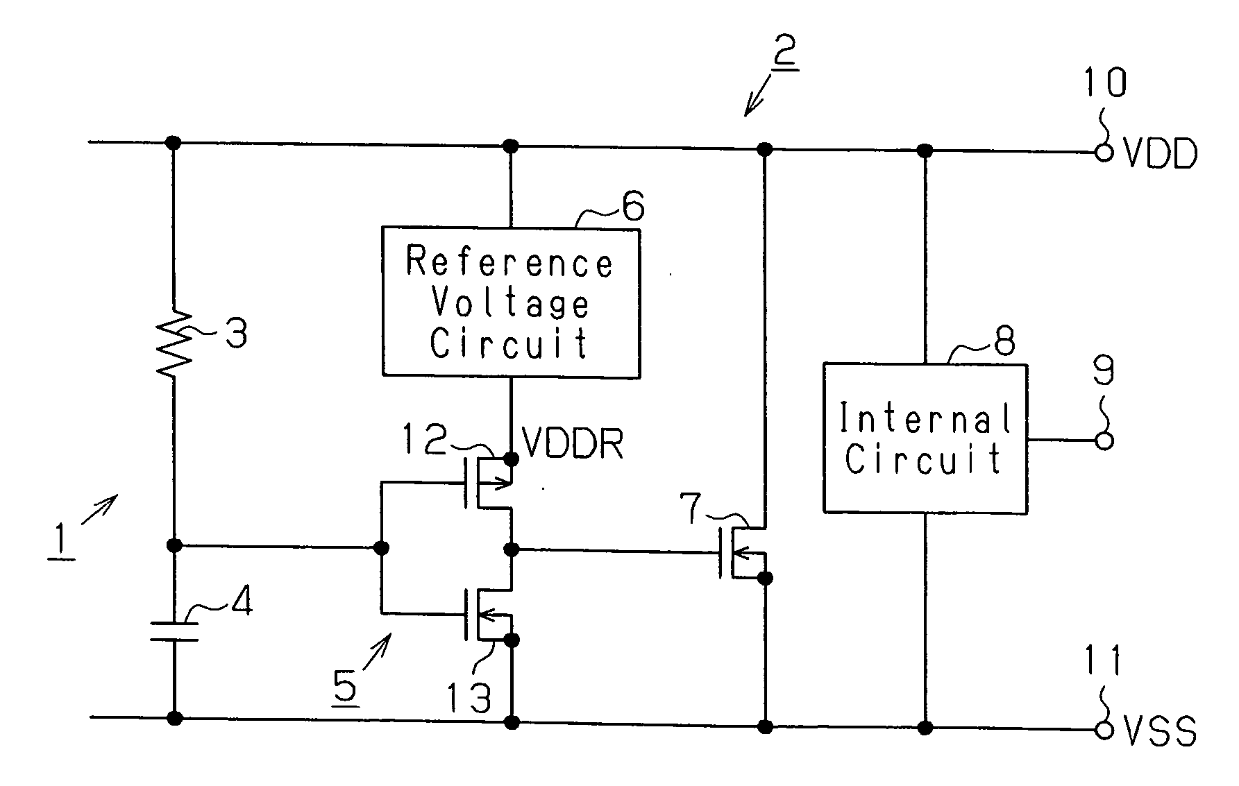
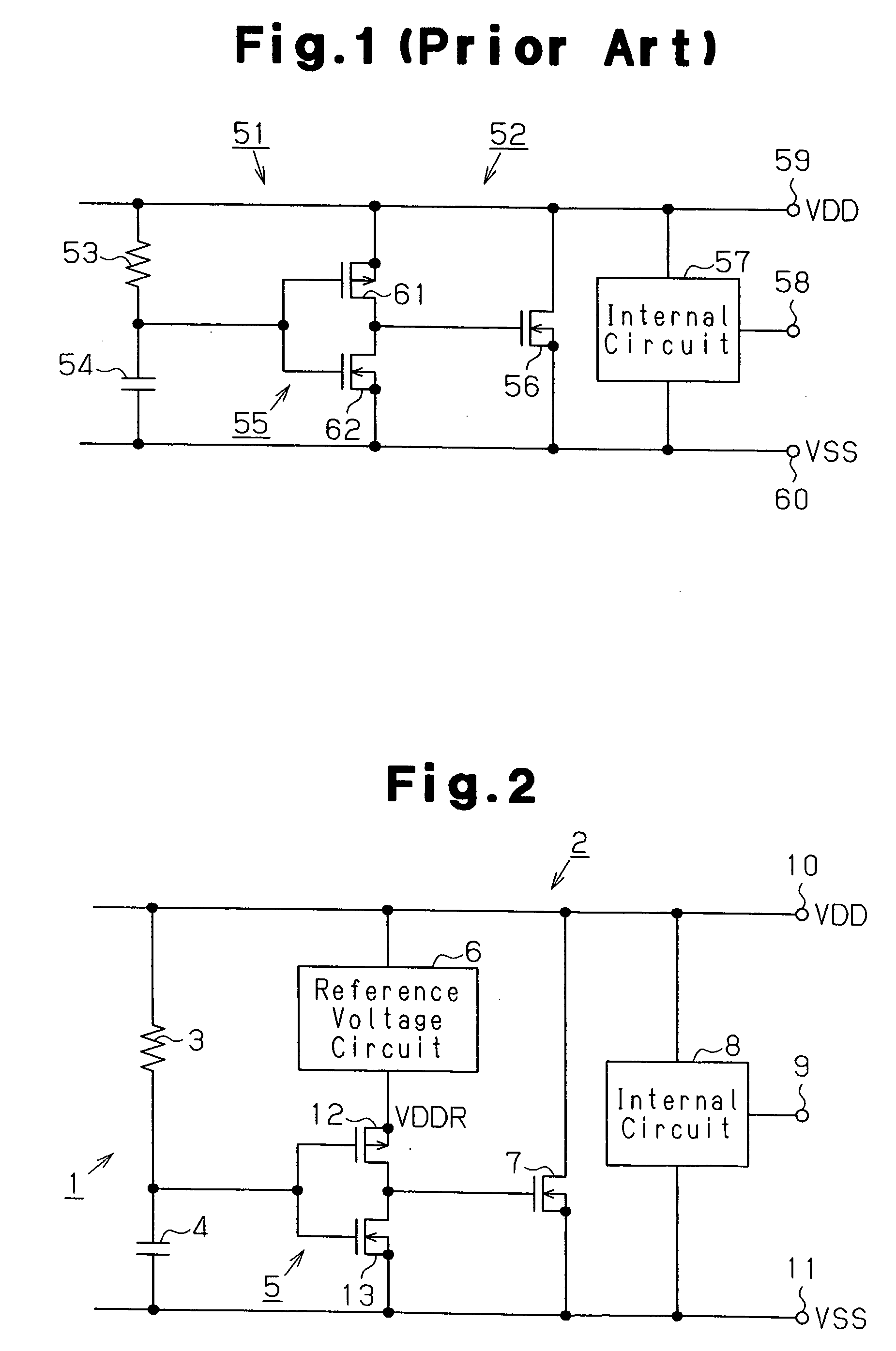
[0027] A semiconductor device 2, which is preferably an LSI, includes the power clamp circuit 1 and an internal circuit 8. The power clamp circuit 1 includes a resistor 3, a capacitor 4, a buffer circuit 5, a reference voltage circuit 6, and an N-channel type MOS transistor 7 functioning as a clamp element. The internal circuit 8 is connected to an I / O terminal 9 for input and output of signals, a first power supply terminal 10 for supplying a first power supply voltage VDD, and a second power supply terminal 11 for supplying a second power supply voltage VSS. The first power supply voltage VDD is a positive voltage, and the second power supply voltage VSS is a negative voltage.

[0028] The resistor 3 and the capacitor 4 are connecte...

second embodiment

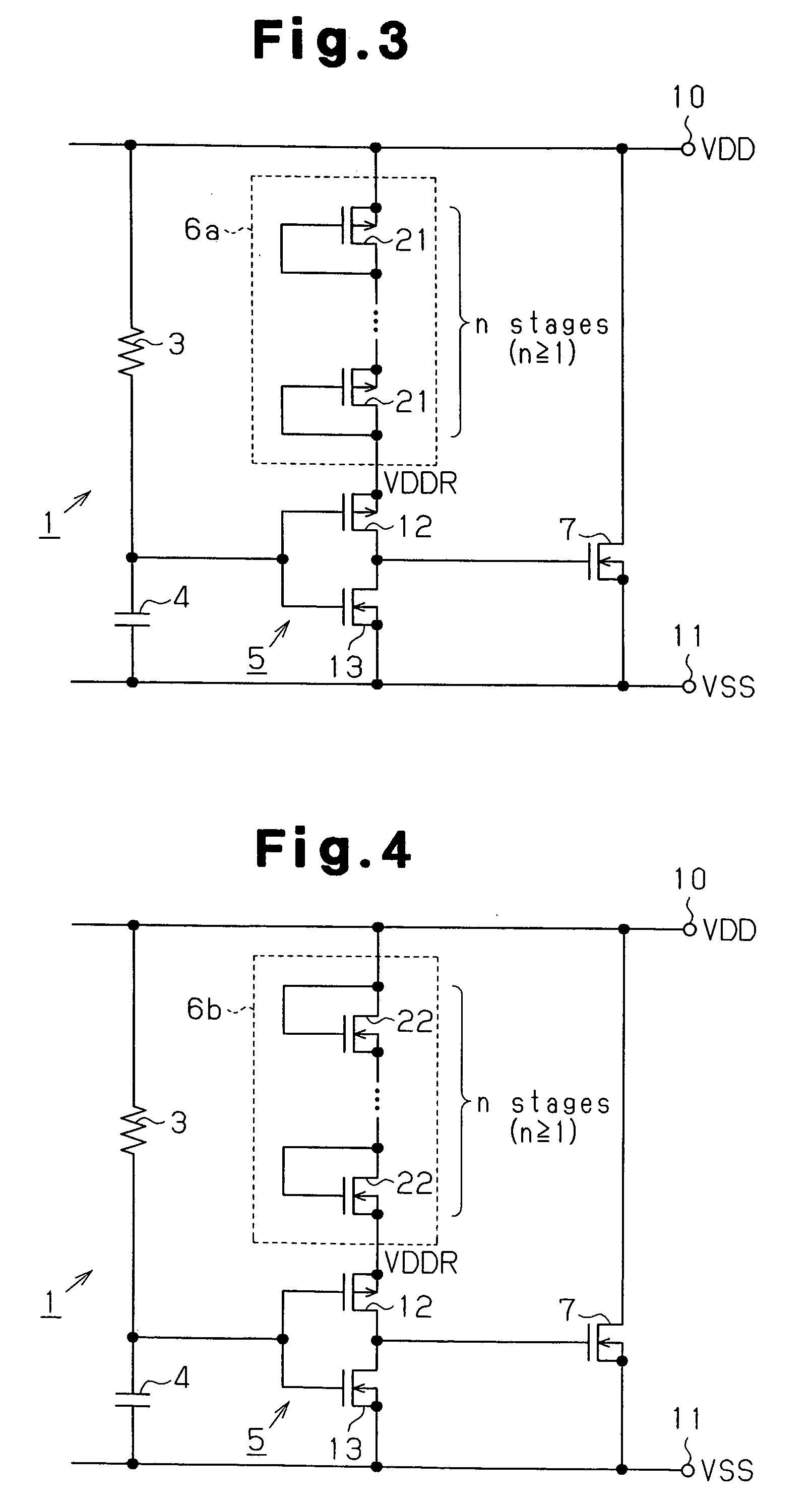
[0041] The power clamp circuit 31 includes (2n−1) stages of (i.e., an odd number of stages satisfying n≧2) buffer circuits 5 and a reference voltage circuit 6a (FIG. 3). The buffer circuits 5 are connected in series between the transistor 7 and a node between the resistor 3 and the capacitor 4. The reference voltage circuit 6a is connected to at least one of the (2n−1) stages of buffer circuits 5 (except for the final buffer circuit). The reference voltage circuit 6a may be replaced by the reference voltage circuit 6b (FIG. 4) or the reference voltage circuit 6c (FIG. 5).

[0042] Each of the buffer circuits 5 is preferably configured by an inverter circuit. In the second embodiment, among the (2n−1) buffer circuits 5, the reference voltage circuit 6a is connected between the first power supply terminal 10 and the source of the first transistor 12 of the (2n−3)th stage of the buffer circuits 5. Thus, the first power supply voltage VDD is directly supplied from the first power supply t...

third embodiment

[0050] A power clamp circuit 41 according to the present invention will now be described with reference to FIG. 8 focusing on the differences from the above embodiments.

[0051] The power clamp circuit 41 counters power supply noise, which may be produced at the side of the second power supply voltage VSS, in a manner similar to the above embodiments. Specifically, the N-channel type MOS transistor 7, which functions as a clamp element, is replaced by a P-channel type MOS transistor 7a, and the reference voltage circuit 6b (see FIG. 4) is connected between the second power supply terminal 11 and the source of the second transistor 13 of the buffer circuit 5. The reference voltage circuit 6b may be replaced by the reference voltage circuit 6a (FIG. 3) or the reference voltage circuit 6c (FIG. 5).

[0052] The power clamp circuit 41 includes 2n stages of buffer circuits 5 (i.e., an even number of stages satisfying n>1), with each buffer circuit being configured by an inverter circuit. At ...


PUM


Abstract

A power clamp circuit for preventing unnecessary power supply leak current at a tolerable power supply noise level. A reference voltage circuit generates a reference voltage by reducing a positive voltage supplied from a first power supply terminal by a predetermined potential and supplies the reference voltage to a buffer circuit. The buffer circuit activates a transistor functioning as a clamp element based on the reference voltage to short-circuit the first and second power supply terminals.

Description

[0001] This application is based upon and claims the benefit of priority from the prior Japanese Patent Application No. 2005-118781, filed on Apr. 15, 2005, the entire contents of which are incorporated herein by reference. BACKGROUND OF THE INVENTION [0002] The present invention relates to a semiconductor device, and more particularly, to a power clamp circuit applicable to an electro-static discharge (ESD) protection circuit for protecting an internal circuit of a semiconductor device from ESD. [0003] A typical semiconductor device (LSI) has an internal circuit configured by miniaturized semiconductor elements. The semiconductor device is therefore provided with a power clamp circuit which functions as a protection circuit for protecting the semiconductor elements from voltage surge caused by external ESD. The power clamp circuit prevents voltage exceeding a tolerable allowable level from being applied to the internal circuit. [0004]FIG. 1 is a schematic circuit diagram showing a ...

Claims


Application Information

Patent Timeline
IPC IPC(8): H03K5/08
CPCH01L27/0285H03K5/08H02H9/046H02H3/20
Inventor IWAHORI, JUNJISUZUKI, TERUOHASHIMOTO, KENJISAITO, NORIAKI
Owner FUJITSU MICROELECTRONICS LTD
Why Eureka
Try Eureka