Method for forming a semiconductor device including a plasma ashing treatment for removal of photoresist

a technology of plasma ashing treatment and semiconductor device, which is applied in the field of semiconductor device including plasma ashing treatment for removal of photoresist, can solve the problem of no effective technique for removing tiox film from the surface of the bottom electrode, and achieve the effect of increasing the capacitan

Inactive Publication Date: 2006-10-19
ELPIDA MEMORY INC
View PDF13 Cites 25 Cited by
  • Summary
  • Abstract
  • Description
  • Claims
  • Application Information

AI Technical Summary

Benefits of technology

[0009] In view of the above, it is an object of the present invention to provide a method for forming a semiconductor device including a MIM capacitor having a higher capacitance by suppressing the oxidation of the bottom electrode in the plasma ashing treatment.
[0011] In accordance with the method of the present invention, the non-oxygen gas in the ashing treatment prevents oxidation of the bottom electrode, thereby suppressing reduction in the film quality of the metal nitride film.
[0012] It is preferable that the non-oxygen gas include N2, NH3, H2 or a mixture of N2 and H2. N2 is most preferable, for reducing the number of crystal defects in the underlying metal nitride film. The reduction of the crystal defects improves the interface between the bottom electrode and the capacitor insulation film, if used in a MIM cylindrical capacitor. This improves the film quality of the capacitor insulation film.
[0013] It is also preferable that the non-oxygen gas be accelerated toward the surface of the semiconductor substrate in a direction normal thereto in the plasma-enhanced ashing treatment. This allows the plasma to effectively reach the bottom portion of the trench, suppressing the occurrence of residues of photoresist. In such a case, it is also preferable that the non-oxygen gas is accelerated using a bias power of 150 watts or above.
[0015] It is also preferable that the method further includes, succeeding to the photoresist removing step, the steps of cooling the semiconductor substrate down to a temperature of 100 degrees C. or lower, and exposing metal nitride film to an atmospheric air. These steps further suppress oxidation of the metal nitride film.

Problems solved by technology

In this case, there is no effective technique for removing the TiOx film from the surface of the bottom electrode in the MIM capacitor.

Method used


Image

  • Method for forming a semiconductor device including a plasma ashing treatment for removal of photoresist
  • Method for forming a semiconductor device including a plasma ashing treatment for removal of photoresist
  • Method for forming a semiconductor device including a plasma ashing treatment for removal of photoresist

Examples


Embodiment Construction

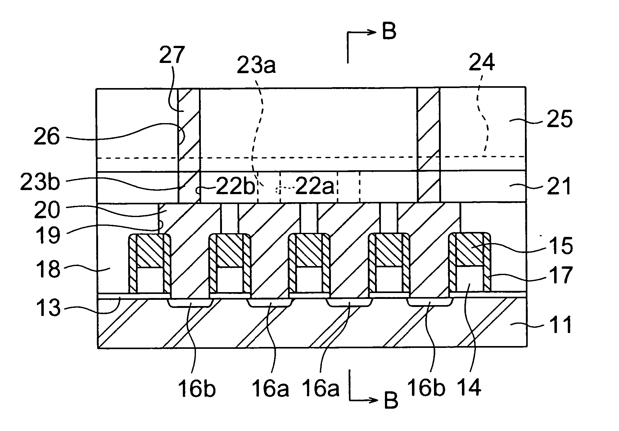
[0024] Now the present invention is described in more detail with reference to accompanying drawings based on a preferred embodiment thereof. FIG. 1A shows a step in a fabrication process for manufacturing a semiconductor device according to the embodiment of the present invention, which is configured as a DRAM device. FIG. 1B is a sectional view taken long line B-B in FIG. 1A.

[0025] In fabrication of the DRAM device, as shown in FIGS. 1A and 1B, an element isolation film 12 is formed in an isolation trench formed on the surface of a silicon substrate 11, thereby isolating the area of the silicon substrate 11 into a plurality of elongate element forming regions. Subsequently, the surface of the silicon substrate 11 is oxidized using a thermal oxidation technique, thereby forming a gate insulation film 13 made of SiO2. Thereafter, materials for the gate electrode 14 and a Si3N4 film 15 are consecutively deposited on the gate insulation film 13 by using a CVD (Chemical Vapor Depositi...


PUM


Abstract

A method for forming a cylindrical capacitor having a metal-nitride bottom electrode, capacitor insulation film and a top electrode in a DRAM device includes the step of forming a photoresist film on the bottom electrode in a cylindrical hole, removing the photoresist film by using a plasma ashing treatment using non-oxygen gas, and consecutively forming the insulation film and the top electrode on the bottom electrode. The plasma ashing treatment uses a bias power for accelerating the plasma gas into the cylindrical trench.

Description

TECHNICAL FIELD [0001] The present invention relates to a method for forming a semiconductor device including a plasma ashing treatment for removal of photoresist and, more particularly, to a method suitably used for forming a MIM (Metal-Insulator-Metal) capacitor having a cylindrical structure in a semiconductor device. BACKGROUND ART [0002] A DRAM device has an increasing number of memory cells by employing a reduced design rule. The reduced design rule inevitably reduces the occupied area of each memory cell, and thus requires a reduced occupied area for a stacked capacitor used in the memory cell without reducing the capacitance thereof. A cylindrical capacitor is generally used as the stacked capacitor for storing data in a memory cell, for achieving a reduced occupied area and yet a larger capacitance. [0003]FIG. 10 shows a conventional cylindrical capacitor, such as described in Patent Publication JP-2002-110674A. The cylindrical capacitor 36 includes a bottom electrode 30 fo...

Claims


Application Information

Patent Timeline
Patent Type & Authority Applications(United States)
IPC IPC(8): H01L21/311
CPCG03F7/427H01L28/91H01L27/10852H01L21/31138H10B12/033
Inventor OHUCHI, MASAHIKO
Owner ELPIDA MEMORY INC
Why Eureka
Try Eureka