Cobalt tungsten phosphate used to fill voids arising in a copper metallization process

a technology of copper metallization and copper phosphate, which is applied in the direction of semiconductor devices, semiconductor/solid-state device details, electrical devices, etc., can solve the problems of reducing the speed of semiconductor circuits, forming voids in copper-filled trenches and vias, and rapidly distributing copper through various materials

Inactive Publication Date: 2006-10-26
SONY CORP +1
View PDF21 Cites 25 Cited by
  • Summary
  • Abstract
  • Description
  • Claims
  • Application Information

AI Technical Summary

Problems solved by technology

One drawback arising from the use of a copper conductor is that copper diffuses rapidly through various materials.
However, these materials have a high dielectric constant, which mean they tend to increase capacitance and thus reduce semiconductor circuit speed.
However, even with the use of a barrier layer, copper is still subject to strong electro-migration, or movement of copper atoms under electrical current which can lead to formation of voids in the copper-filled trenches and vias.
Unfortunately, the cap layer, which is typically silicon nitride or silicon carbide, undesirably increases the dielectric constant of the structure.

Method used


Image

  • Cobalt tungsten phosphate used to fill voids arising in a copper metallization process
  • Cobalt tungsten phosphate used to fill voids arising in a copper metallization process
  • Cobalt tungsten phosphate used to fill voids arising in a copper metallization process

Examples


Embodiment Construction

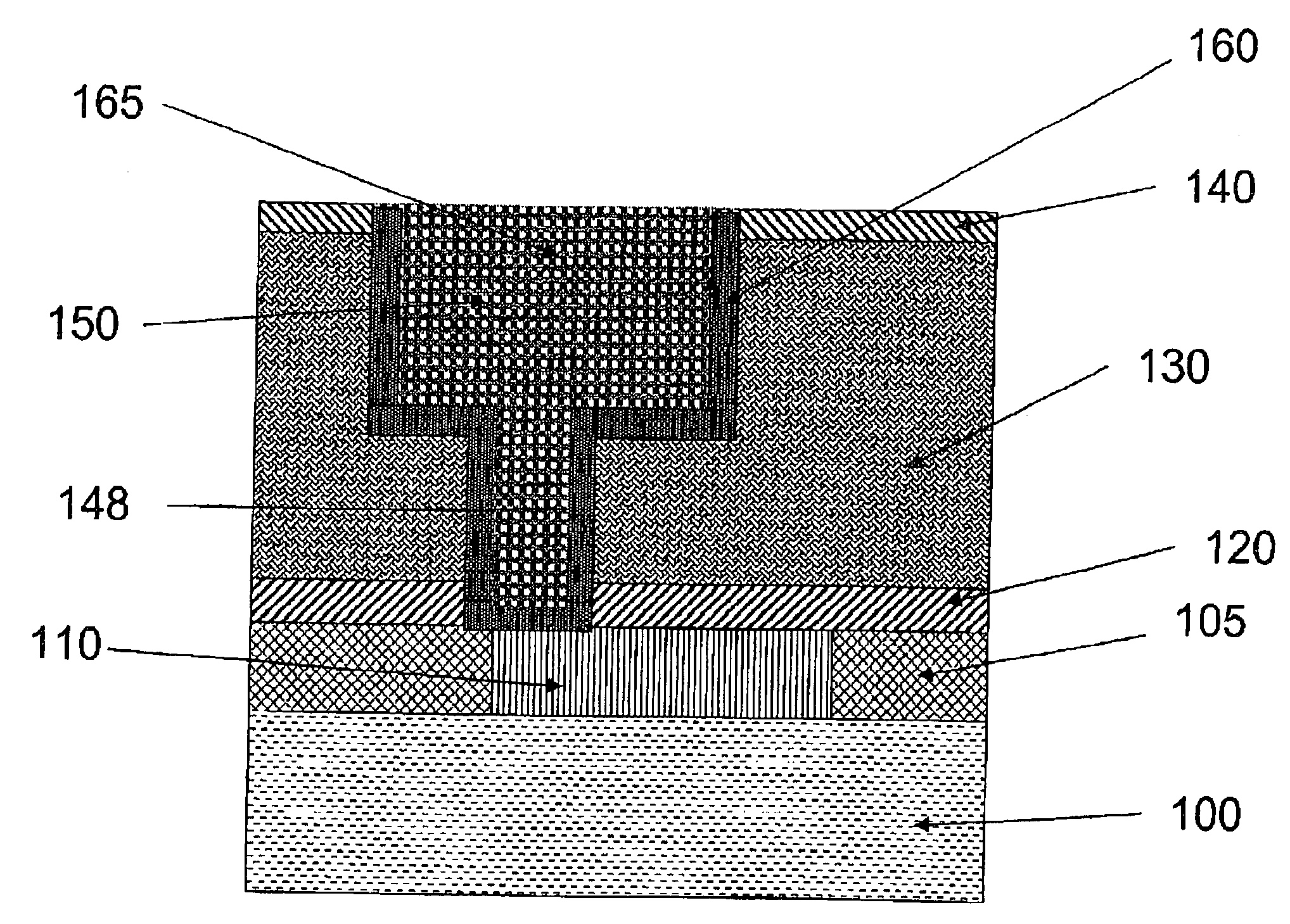
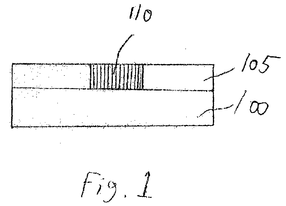
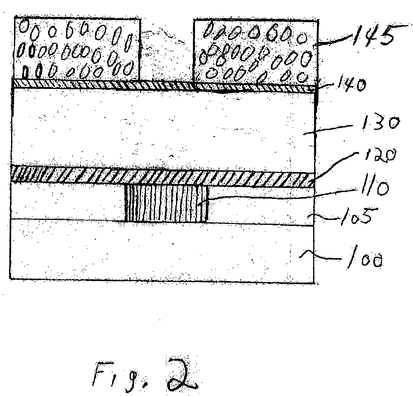
[0024] The methods and structures described herein do not form a complete process for manufacturing semiconductor device structures. The remainder of the process is known to those of ordinary skill in the art and, therefore, only the process steps and structures necessary to understand the present invention are described herein.

[0025] The present invention can be applied to microelectronic devices, such as highly integrated circuit semiconductor devices, processors, micro electromechanical (MEM) devices, optoelectronic devices, and display devices. In particular, the present invention is highly useful for devices requiring high-speed characteristics, such as central processing units (CPUs), digital signal processors (DSPs), combinations of a CPU and a DSP, application specific integrated circuits (ASICs), logic devices, and SRAMs.

[0026] In the present invention a barrier layer is formed between multilayer interconnections without the need to subsequently form a thick cap layer tha...


PUM

PropertyMeasurementUnit
thicknessaaaaaaaaaa
thicknessaaaaaaaaaa
dielectric constantaaaaaaaaaa

Abstract

A semiconductor device includes a substrate, at least one layer of functional devices formed on the substrate, a first dielectric layer formed over the functional device layer and a first trench / via located in the first dielectric layer. A copper conductor fills the first trench / via. An electromigration inhibiting barrier layer is selectively located over a surface of the copper conductor and not any other remaining exposed surface. An insulating cap layer overlies the barrier layer and the remaining exposed surface. A second dielectric layer overlies the insulating cap layer. A second trench / via is located in the second dielectric layer and extends through the insulating cap layer and the barrier layer. A micro-trench is located within the first dielectric layer and is associated with the formation of the second trench / via. The micro-trench exposes a portion of the copper conductor. A filler fills the micro-trench. The filler is formed from a material used to form the electromigration inhibiting barrier layer.

Description

FIELD OF THE INVENTION [0001] The present invention relates generally to dual damascene interconnections for integrated circuits, and more specifically to a dual damascene interconnection in which the cap layer can be reduced in thickness when a barrier layer is employed between multilayer metal interconnections. BACKGROUND OF THE INVENTION [0002] The manufacture of integrated circuits in a semiconductor device involves the formation of a sequence of layers that contain metal wiring. Metal interconnects and vias which form horizontal and vertical connections in the device are separated by insulating [0003] layers or inter-level dielectric layers (ILDs) to provide electrical insulation between metal wires and prevent crosstalk between the metal wiring that can degrade device performance. [0004] A popular method of forming an interconnect structure is a dual damascene process in which vias and trenches are filled with metal in the same step to create multi-level, high density metal in...

Claims


Application Information

Patent Timeline
Patent Type & Authority Applications(United States)
IPC IPC(8): H01L23/52
CPCH01L21/76808H01L21/76843H01L21/76849H01L21/76852H01L21/76868H01L2924/0002H01L23/5226H01L23/53238H01L2924/00
Inventor NOGAMI, TAKESHI
Owner SONY CORP
Why Eureka
Try Eureka