Method for manufacturing gallium nitride-based semiconductor device

a gallium nitride and semiconductor technology, applied in the direction of semiconductor devices, basic electric elements, electrical appliances, etc., can solve the problems of many defects such as dislocation, not widely available, and the substrate material for growing the gan-based single crystal is not suitable for use, so as to improve the crystalinity of the gan-based semiconductor. , the effect of inhibiting the occurrence of crystalline defects

Inactive Publication Date: 2006-11-02
SAMSUNG ELECTRO MECHANICS CO LTD
View PDF4 Cites 24 Cited by
  • Summary
  • Abstract
  • Description
  • Claims
  • Application Information

AI Technical Summary

Benefits of technology

[0012] The present invention has been made to solve the foregoing problems of the prior art and it is therefore an object of the present invention to provide a method for manufacturing a GaN-based semiconductor capable of inhibiting occurrence of crystalline defects and further improving crystalinity of the GaN-based semiconductor.

Problems solved by technology

However, problematically, a substrate material for growing the GaN-based single crystal, which matches lattice constant and thermal expansion coefficient of the GaN-based single crystal, has not been commonly available.
But due to big lattice mismatch between the hetero-substrate such as the sapphire substrate and the GaN single crystal (e.g., about 18% lattice mismatch between the sapphire substrate and GaN single crystal), the growth of the GaN-based semiconductor layer on the hetero-substrate leads to many defects such as dislocation.
However, despite use of the buffer layer, crystalline defects inevitably arise due to considerable lattice mismatch between the hetero-substrate such as the sapphire substrate and the GaN-based semiconductor.
For example, even in case of using the low-temperature GaN buffer layer, it generates crystalline defects of about 1010 / cm3, thereby hindering manufacture of a high-quality light emitting device such as Light Emitting Diodes (LEDs) or Laser Diodes (LDs).
In addition, conventional methods are not appropriate for growing a bulk-type GaN-based semiconductor thick film having a thickness of more than tens of μm.

Method used


Image

  • Method for manufacturing gallium nitride-based semiconductor device
  • Method for manufacturing gallium nitride-based semiconductor device
  • Method for manufacturing gallium nitride-based semiconductor device

Examples


Embodiment Construction

[0032] The present invention now will be described more fully hereinafter with reference to the accompanying drawings, in which preferred embodiments of the invention are shown. This invention may, however, be embodied in many different forms and should not be construed as limited to the embodiments set forth herein. Rather, these embodiments are provided so that this disclosure will be thorough and complete, and will fully convey the scope of the invention to those skilled in the art. In the drawings, the shapes and dimensions may be exaggerated for clarity, and the same reference signs are used to designate the same or similar components throughout.

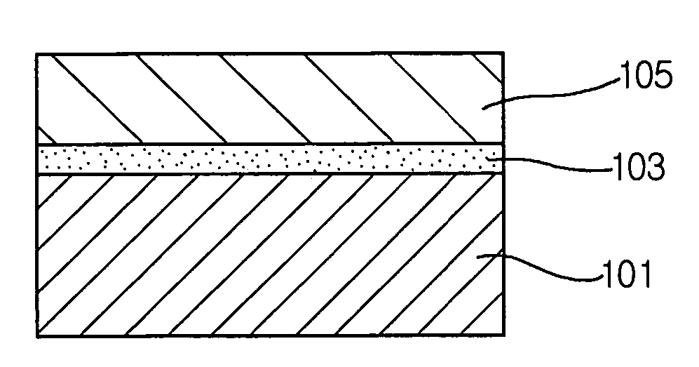
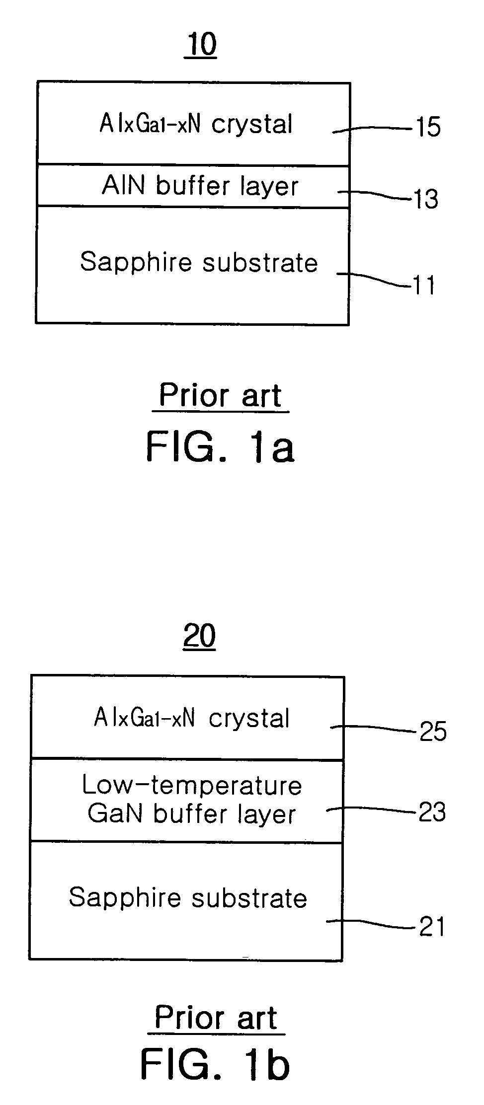
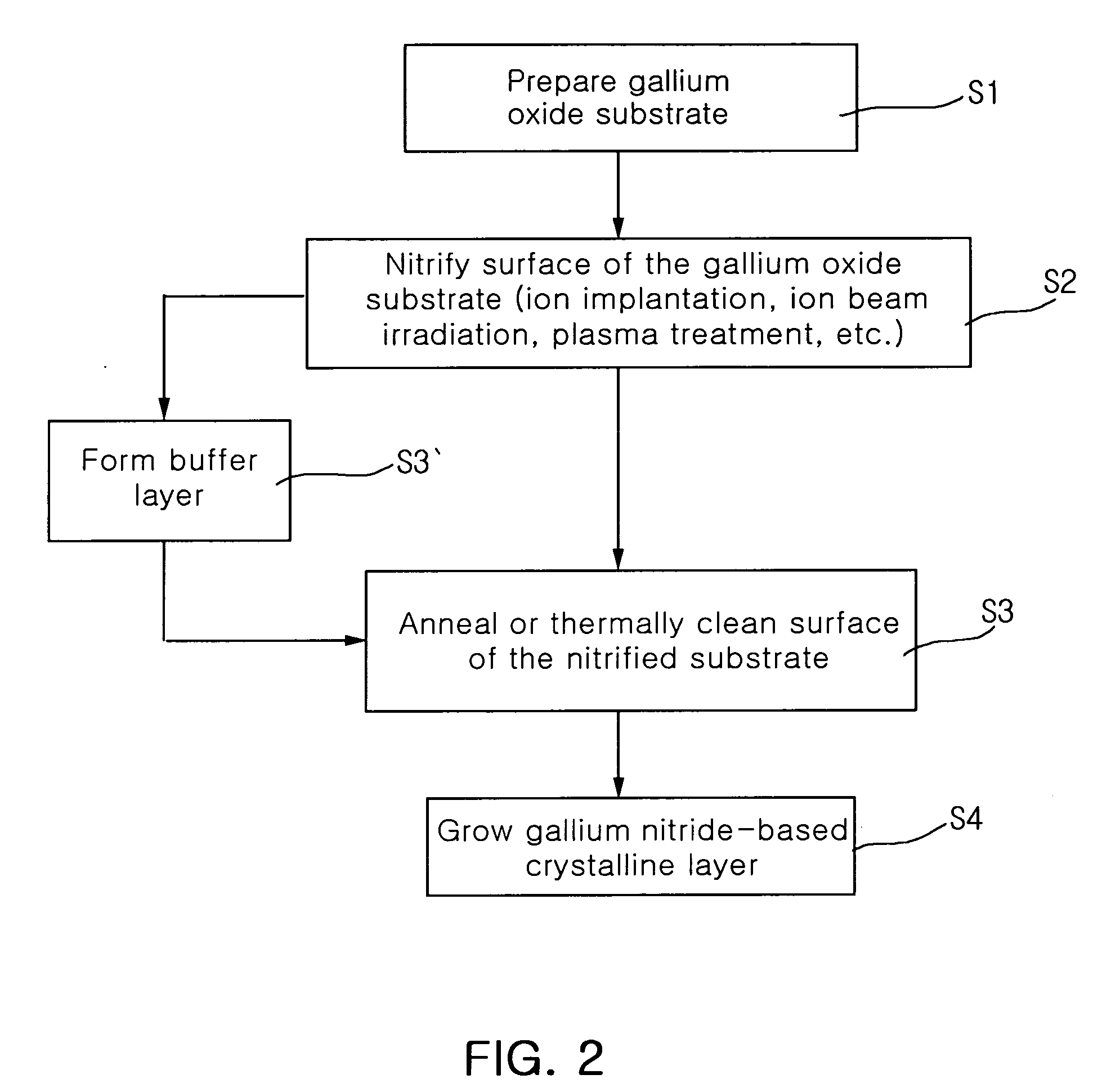
[0033]FIG. 2 is a schematic flow chart illustrating a method for manufacturing a GaN-based semiconductor according to the invention. Referring to FIG. 2, first, a gallium oxide substrate such as a LiGaO2 substrate or a Ga2O3 substrate is prepared in S1. The gallium oxide substrate exhibits much higher lattice match with a GaN crystal t...


PUM

PropertyMeasurementUnit
energyaaaaaaaaaa
energyaaaaaaaaaa
temperatureaaaaaaaaaa

Abstract

The invention provides a method for manufacturing a gallium nitride-based semiconductor device having low-density crystalline defects and high-quality crystalinity. In the manufacturing method according to the invention, first, a gallium oxide substrate is prepared. Then, a surface of the gallium oxide substrate is modified into a nitride via physical or chemical pretreatment to form a surface nitride layer having Ga—N bonding. Finally, gallium nitride-based semiconductor layer is formed on the surface nitride layer.

Description

RELATED APPLICATION [0001] This application claims the benefit of Korean Patent Application No. 2005-36571 filed on Apr. 30, 2005 in the Korean Intellectual Property Office, the disclosure of which is incorporated herein by reference. BACKGROUND OF THE INVENTION [0002] 1. Field of the Invention [0003] The present invention relates to a method for manufacturing a gallium nitride-based semiconductor. More particularly, the present invention relates to a method for manufacturing a gallium nitride-based semiconductor which ensures a GaN-based semiconductor layer with high-quality crystalinity. In the specification, a GaN-based semiconductor designates a binary, ternary or quaternary compound semiconductor having a composition expressed by AlxGayIn(1-X-y)N, where 0≦x≦1, 0≦y≦1, and 0≦x+y≦1. [0004] 2. Description of the Related Art [0005] Recently, a GaN-based semiconductor has garnered attention as a material that can be suitably applied to an opto electronic device of a short wavelength ...

Claims


Application Information

Patent Timeline
Patent Type & Authority Applications(United States)
IPC IPC(8): H01L21/00H01L33/12H01L33/32
CPCH01L21/02414H01L21/0242H01L21/02658H01L21/0254H01L21/02458H01L21/20
Inventor SUH, HYO WON
Owner SAMSUNG ELECTRO MECHANICS CO LTD
Why Eureka
Try Eureka