Improved free space optical bus

a free space, optical bus technology, applied in multiplex communication, wireless communication, polarisation/directional diversity, etc., can solve the problems of increasing the handicap of rapid improvement of the ability to process data within a chip or computer or network element, the i/o elements of electrical chips do not scale according to moore's law, and the limitations of electrical communication, etc., to achieve the effect of ensuring the transmission quality of the bus

Inactive Publication Date: 2006-11-09
BEN GURION UNIVERSITY OF THE NEGEV
View PDF71 Cites 62 Cited by
  • Summary
  • Abstract
  • Description
  • Claims
  • Application Information

AI Technical Summary

Benefits of technology

[0012] The present invention seeks to provide new methods for improving the quality of optical free space connections in optical bus-systems between circuitry elements in high speed computing, communication and signal processing systems. The methods are applicable to any free space optical buses, whether on a nano-scale, such as in intra- or inter-chip communication requirements in computing systems, in medium scale applications between boards or computers, or on a macro-scale, such as in a cluster of supercomputers or in the potentially noisy environment of aircraft, landcraft, spacecraft or seacraft. Additionally, the methods of the present invention may generally be used on conventional optical bus systems, without amending any of the intrinsic functional operation of the computer system components, and generally only requiring the addition of electronic or optical processing functions or modules to the bus system.
[0017] There is thus provided in accordance with a preferred embodiment of the present invention, a a method of improving the transmission quality of a free-space optical bus system comprising the steps of: (i) providing an optical bus having a plurality of transmitters and receivers connected by optical paths, (ii) transmitting a signal onto the bus from one of the transmitters, (iii) measuring the signal received by at least some of the receivers, (iv) repeating the steps of transmitting and measuring for additional ones of the transmitters, (v) utilizing the measured signals to generate a transmission quality function for the bus, and (vi) optimizing the transmission quality function by adjusting at least one characteristic associated with transmission along at least one of the paths.
[0019] In accordance with yet another preferred embodiment of the present invention, in the above described method the transmission quality of the bus is ascertained by measuring the transmission bit error rate along at least some of the optical paths. Furthermore, the transmission quality improvement is able to counteract the effects of at least one of mechanical and thermal environmental effects on the bus.
[0033] In accordance with yet another preferred embodiment of the present invention, in such a free space optical bus system each of the links may preferably have a predetermined functionality, at least one of the functionalities comprising at least two different parts, and each of the different parts is preferably transmitted using a different wavelength, such that part selection may be made by selection of transmission wavelength. In such a case, the different parts may be any one of different memory blocks and different input / output groups. Consequently, this wavelength selection enables chip select operations to be performed in the optical domain.

Problems solved by technology

However, this rapidly improving ability to process data within a chip or computer or network element is increasingly handicapped by the failure to provide communication over the bus at a similarly scaled rate.
The problem is that electrical chip I / O elements do not scale according to Moore's Law.
More recently, the bus has sometimes been implemented by means of a bundle of wires but this still has the limitations of electrical communication.
Fiber optical buses do provide increase in performance, but still have physical disadvantages.
For electrical technology, the primary limitations to implementing high-speed interconnections are achieving high packing density, cross talk between channels, frequency-dependent loss, and high power dissipation.
Current optoelectronic technologies, which are optimized for long distance telecommunication and data communication applications, do not have the necessary characteristics (power dissipation, form factor, cost, signal integrity) needed for interconnects between high-speed electronic chips.
However, the optical bus configurations described therein have a number of operative disadvantages.
Environmental conditions and physical limitations reduce the optical bus performance, and increase the noise and interference levels.
Environmental conditions could be thermal bending or turbulence due to non-uniform heating of components, vibration, jitter and impact from external and internal sources, such as cooling fans, aircraft vibration, motor vibration, non-linearity if the propagation medium is not air, scattering of light by small particulate material in the media, and straying light due to non-perfect optics.
The physical limitation could be, for example, diffraction of the transmitted light, generating interference with neighbor links.

Method used


Image

  • Improved free space optical bus
  • Improved free space optical bus
  • Improved free space optical bus

Examples


Embodiment Construction

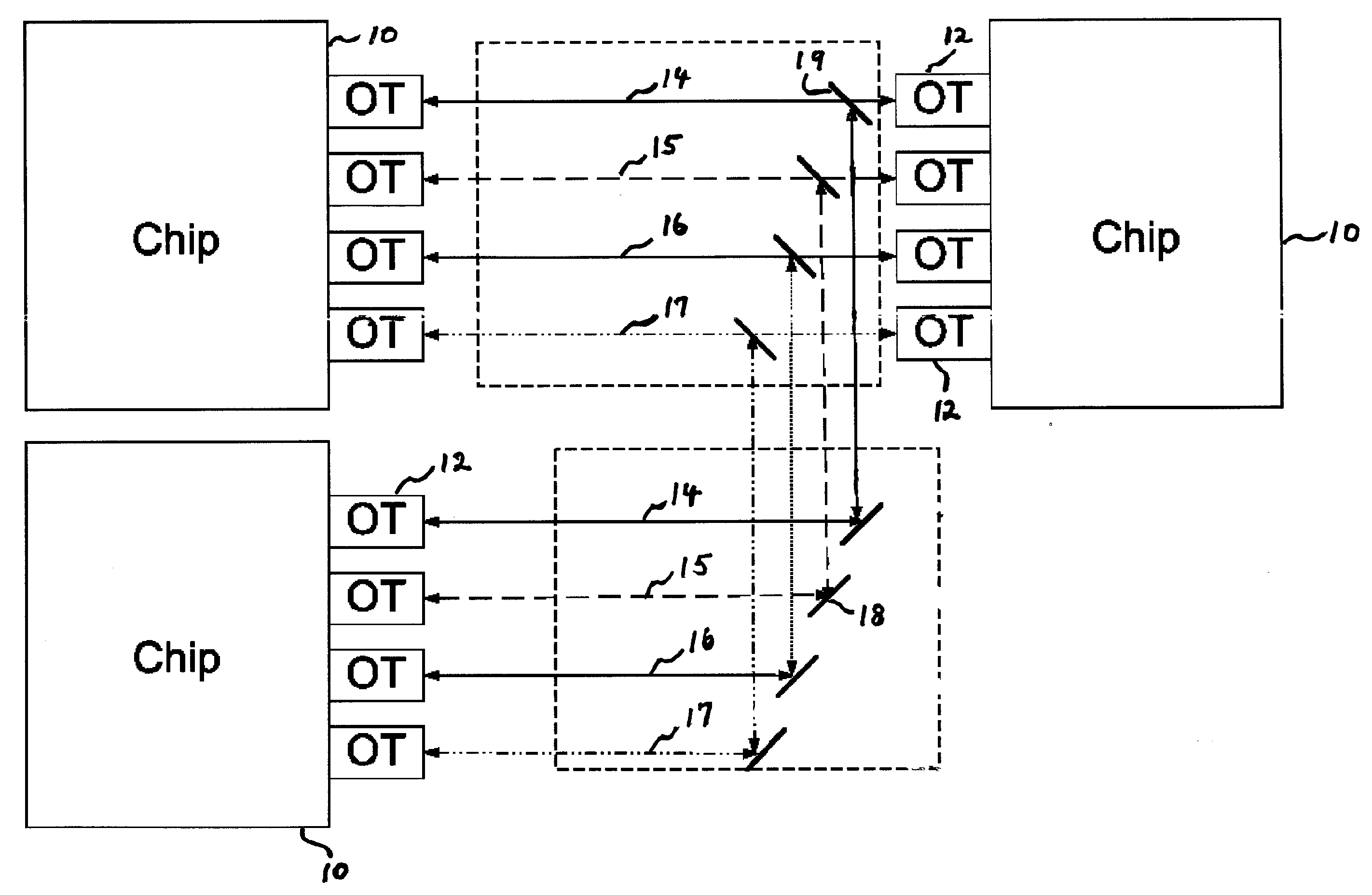
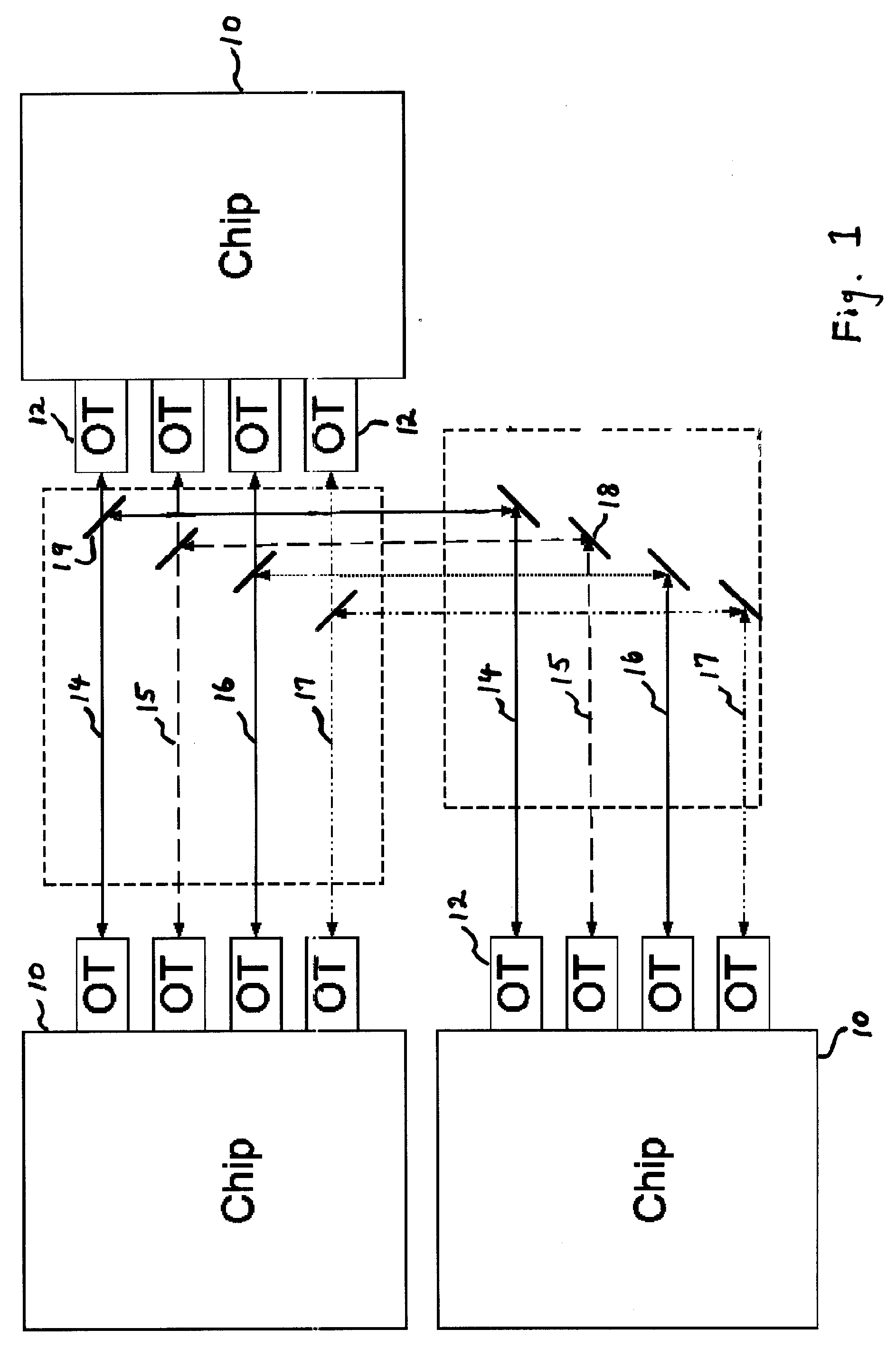
[0052] Reference is now made to FIG. 1, which illustrates schematically an optical wireless bus implemented to communicate, using the preferred methods of the present invention, between the various chips 10 of a computing system. Although only three chips are shown in FIG. 1, it is to be understood that the methods of the present invention are applicable on buses connecting any number of chips. The input / output functions of each of the chips are preferably implemented by means of optical transceivers OT, marked as items 12, though it is to be understood that separate receivers and transmitters may equally well be used. The communication lines between the various chips are implemented by means of optical transmission paths, and may be any of control lines 14, address lines 15, data lines 16 or any other auxiliary lines 17. Spatial redirection of the optical information may preferably be performed by means of arrays of mirrors 18, or, where signal splitting is required to direct the s...


PUM


Abstract

A method and apparatus for improving the transmission quality of a free space optical bus between circuitry elements in high speed computing, communication and signal processing systems. Use is made of an adaptive algorithm that learns the transmission properties of the bus, and selects or adjusts transmission paths or characteristics to provide optimum bus performance. Each transmitter on the bus transmits a signal which is generally measured by all of the receivers on the bus, and the measured signals are used to generate a matrix which maps desired transmission along information links, and cross-link interference. Transmission quality is optimized by adjusting one or more characteristics associated with transmission along the bus, including emitted power, beam divergence, wavelength, beam polarization, antenna gain and antenna polar diagram of the transmitters, and power sensitivity, gain, equalizer coefficients, field of view, polarization sensitivity, antenna gain and antenna polar diagram of the receivers. Novel bus configurations are described, including use of different wavelengths for different bus functions.

Description

[0001] This application claims the benefit and priority of U.S. Provisional Patent Application No. 60 / 678,804 filed on May 9, 2005, the full disclosure of which is hereby incorporated by reference.FIELD OF THE INVENTION [0002] The present invention relates to the field of optical buses for communication between electronic circuits, especially computer or network buses utilizing free space propagation. BACKGROUND OF THE INVENTION [0003] A bus can be described as a subsystem that transfers data and / or power between components or circuits inside a computer, or between computers, or between network elements. In most cases, a computer bus is implemented using conductors on printed circuit boards, or PCBs. PCB's are used to mechanically support and electrically connect electronic components using conductive pathways, or traces, etched from copper sheets laminated onto a non-conductive substrate. Historically, line widths on electronic chips have constantly been reduced, as projected by Go...

Claims


Application Information

Patent Timeline
Patent Type & Authority Applications(United States)
IPC IPC(8): H04J14/00
CPCH04B7/10H04B10/114H04B10/1143H04B10/801H04W40/00H04W16/14H04W24/00H04W28/18H04J14/02
Inventor ARNON, SHLOMI
Owner BEN GURION UNIVERSITY OF THE NEGEV
Why Eureka
Try Eureka