Technique for defining a wettable solder joint area for an electronic assembly substrate

a technology of electronic assembly and solder joint, which is applied in the direction of non-electric welding apparatus, manufacturing tools, and soldering devices, etc., can solve the problems of insufficient use of solder stops, inability to connect conductors to fine-pitch integrated circuit chips, and significant impact on the minimum conductor width of multi-sided solder stops, etc., to achieve the effect of printing and firing traditional solder stops, additional material and processing steps

a technology of electronic assembly and solder joint, which is applied in the direction of non-electric welding apparatus, manufacturing tools, and soldering devices, etc., can solve the problems of insufficient use of solder stops, inability to connect conductors to fine-pitch integrated circuit chips, and significant impact on the minimum conductor width of multi-sided solder stops, etc., to achieve the effect of printing and firing traditional solder stops, additional material and processing steps

US20060255102A1Inactive Publication Date: 2006-11-16DELPHI TECH INC

Image

  • Technique for defining a wettable solder joint area for an electronic assembly substrate
  • Technique for defining a wettable solder joint area for an electronic assembly substrate
  • Technique for defining a wettable solder joint area for an electronic assembly substrate

Examples


Embodiment Construction

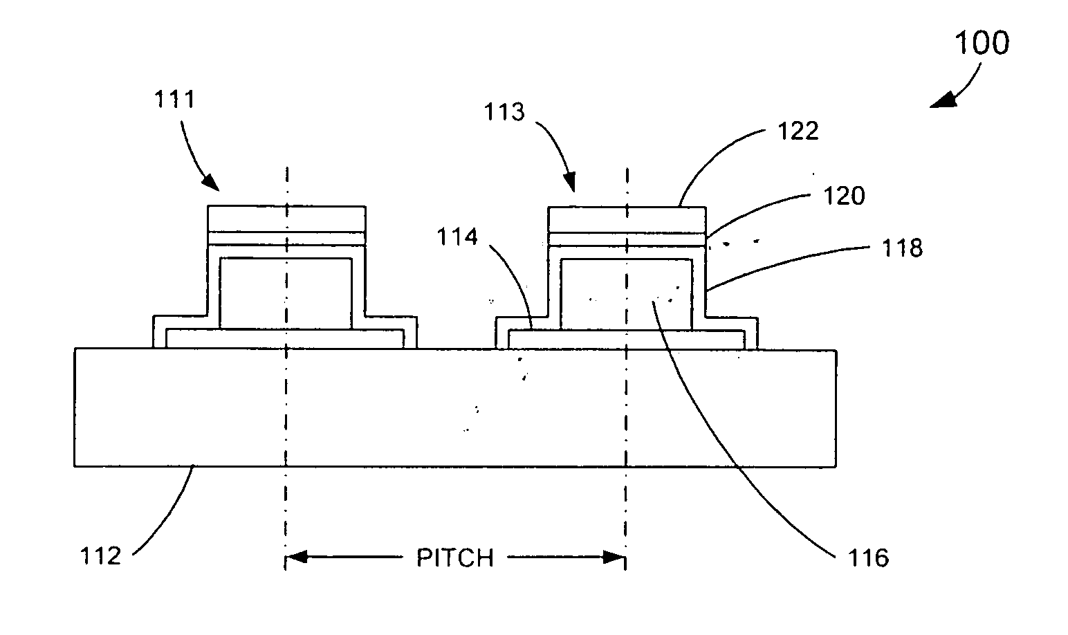
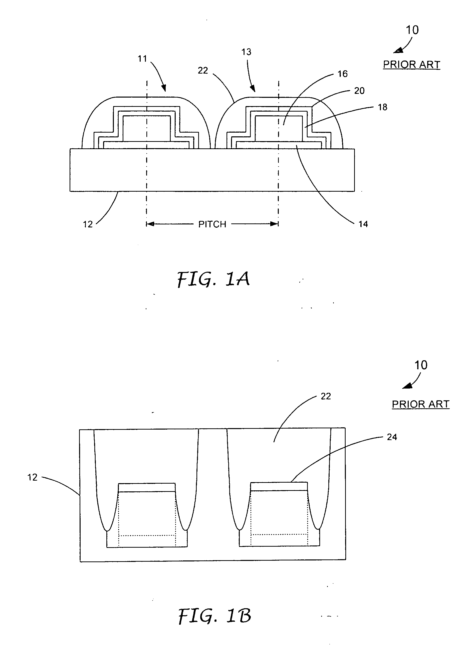
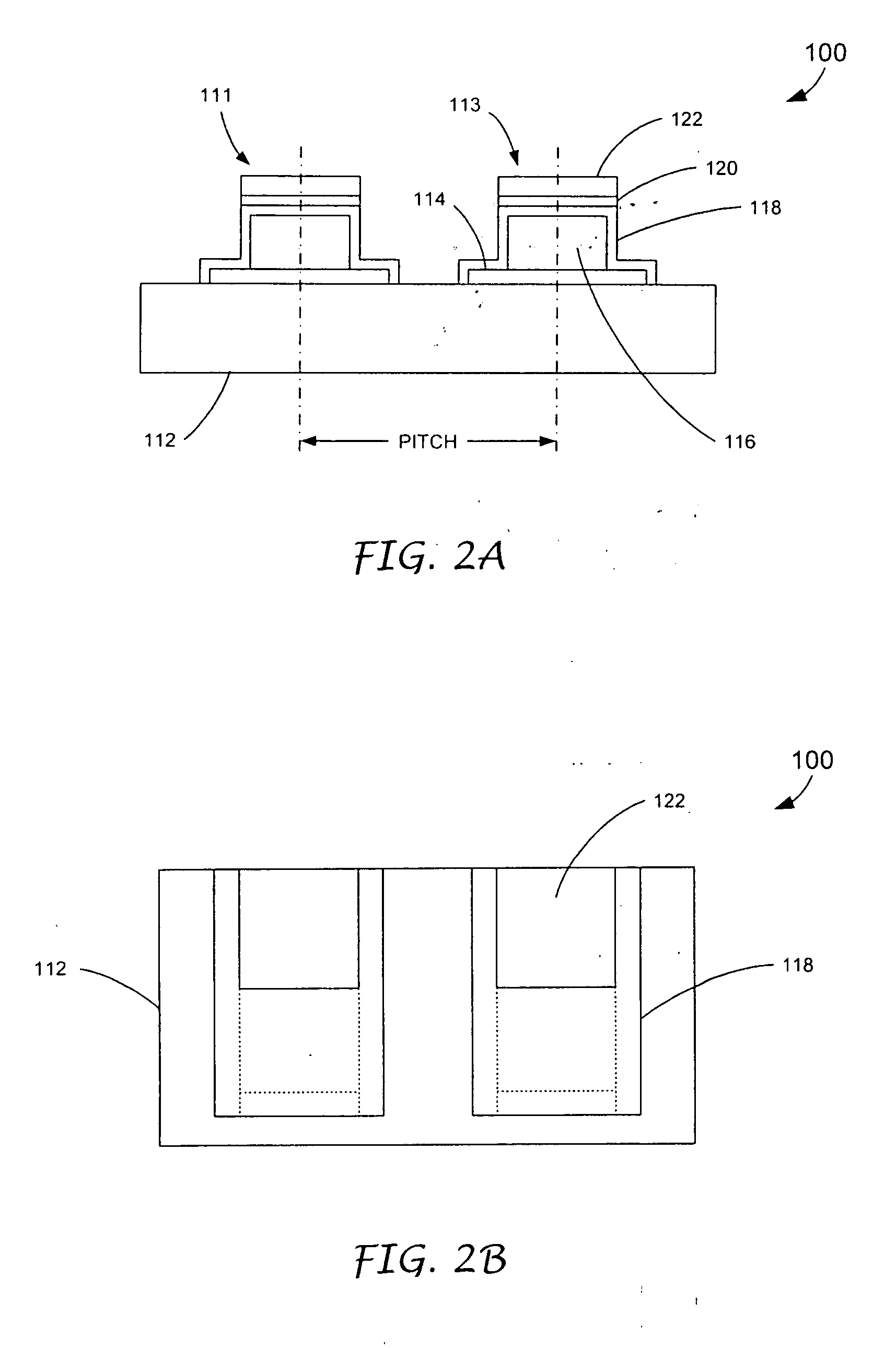
[0022] According to the present invention, a technique is disclosed herein that provides an alternative to typical printed solder stops. According to one aspect of the present invention, an electroless nickel-gold finish, which is a standard finish for copper on ceramic and has become increasingly popular for thick film conductors, is utilized. In a typical electronic assembly that utilizes thick films, a layer of palladium (Pd) is typically deposited between the nickel (Ni) and gold (Au) layers. Typical assemblies include a common base conductor layer, e.g., a copper layer, a nickel layer and a common final layer, typically of gold (Au), which is highly solderable. It should be appreciated that nickel oxidizes relatively easily and does not wet to solder in the oxidized state. According to the present invention, the oxidized nickel (or passivated nickel) is utilized to define a wettable solder joint area for an electronic assembly. Thus, according to the present invention, a zero f...


PUM

PropertyMeasurementUnit
Electrical conductoraaaaaaaaaa
Areaaaaaaaaaaa
Wettabilityaaaaaaaaaa

Abstract

A technique for defining a wettable solder joint area for an electronic assembly reduces and / or dispenses with the use of polymer solder masks. According to the technique, a substrate is provided that includes at least one conductive trace. A nickel layer is provided on the conductive trace and gold is selectively applied on the nickel layer in a desired pattern to form a gold layer. An exposed portion of the nickel layer that does not include the gold in the desired pattern is then oxidized. Finally, a solder is applied to the gold layer, with the oxidized nickel layer providing a solder stop and defining a wettable solder joint area.

Description

TECHNICAL FIELD [0001] The present invention is generally directed to an electronic assembly and, more specifically, to a technique for defining a wettable solder joint area for an electronic assembly substrate. BACKGROUND OF THE INVENTION [0002] Traditionally, solder stops (i.e., solder masks) have been printed onto a substrate to define wettable solder joint areas. Unfortunately, the utilization of a solder stop may be insufficient to avoid wicking of the solder along side-walls of conductors formed on outer surfaces of the substrate. For example, various electronic assemblies that have utilized thermally conductive ceramic substrates, with thick copper conductors or thick film conductors, have experienced solder wicking along side-walls of the conductors. Further, while a single-sided solder stop may be replaced with a multi-sided solder stop, e.g., a four-sided solder stop made of a printed thick film, utilization of a multi-sided solder stop may significantly impact the minimum...

Claims


Application Information

Patent Timeline
16 Nov 2006
Publication
US20060255102A1
IPC
B23K1/20; B23K31/00
CPC
H01L23/498; H01L24/10; H01L24/13; H01L2924/014; H01L2924/01047; H01L2924/00013; H05K2203/0315; H05K2201/2081
Inventors
SNYDER, RICK B.; DELHEIMER, CHARLES I.