Organic electroluminescence device and organic electroluminescence system

Active Publication Date: 2006-11-16
SAMSUNG DISPLAY CO LTD +1
View PDF7 Cites 29 Cited by
  • Summary
  • Abstract
  • Description
  • Claims
  • Application Information

AI Technical Summary

Benefits of technology

[0059] The present invention provides the following means for pr

Problems solved by technology

These approaches, however, do not consider the degradation mechanism of how the or

Method used


Image

  • Organic electroluminescence device and organic electroluminescence system
  • Organic electroluminescence device and organic electroluminescence system
  • Organic electroluminescence device and organic electroluminescence system

Examples


example 1

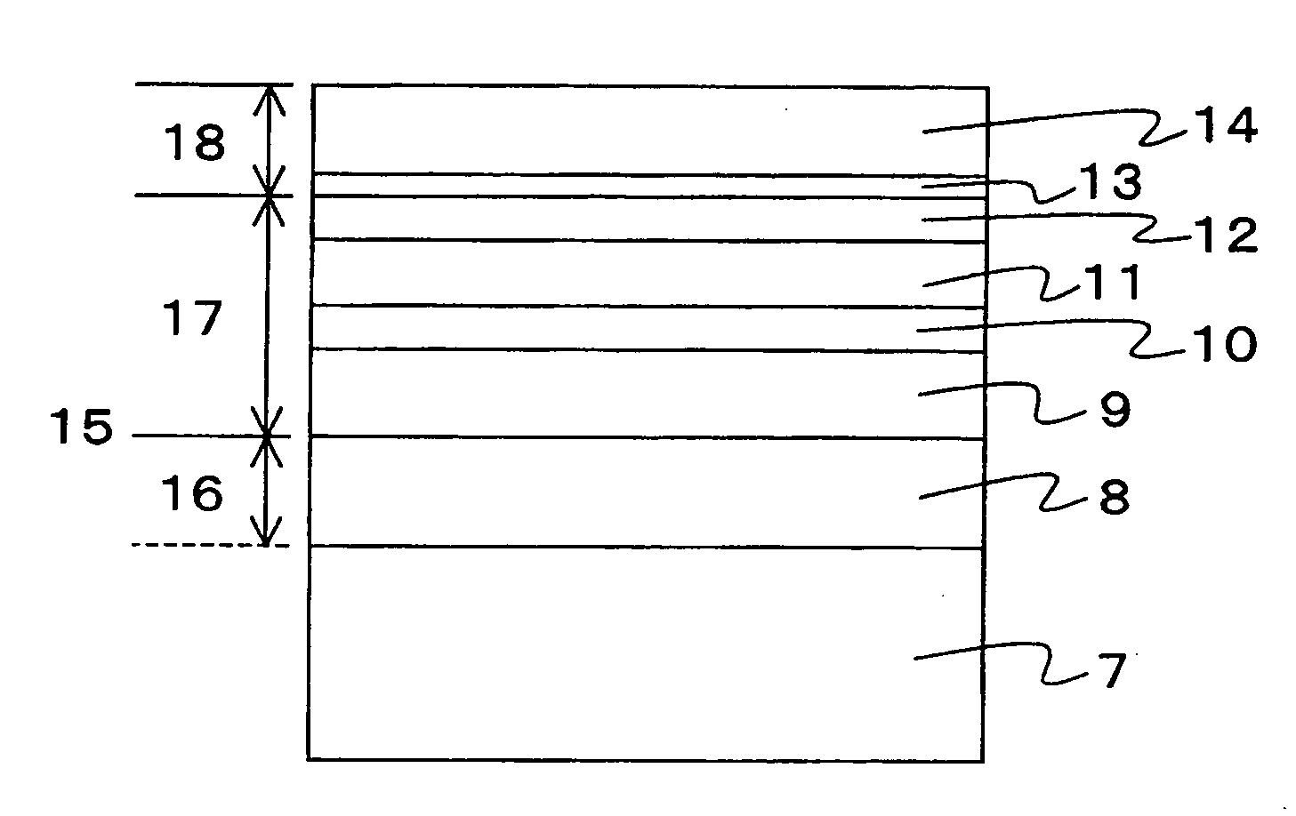
[0151] First, description will be made of the basic structure of an organic electroluminescence device according to the present invention.

[0152]FIG. 1(a) shows the basic structure of the organic electroluminescence device according to the present invention. The organic electroluminescence device is formed on a substrate (1). By way of example, a metal oxide electrode (2) is formed immediately above the substrate (1).

[0153] A thin film layer (5) containing an organic substance is formed on the metal oxide electrode (2). A second electrode (6) different from the metal oxide electrode (2) is formed on the layer (5).

[0154] The organic substance-containing thin film layer (5) is shown as a single layer in FIG. 1(a) for simplicity. In reality, however, it may be formed as a multi-layered structure consisting of various thin films (such as an organic thin film, an inorganic thin film, and an organic-inorganic composite thin film) as known in many organic electroluminescence devices.

[01...

example 2

[0256] Next, description will be made of the results of the examinations similar to those in Embodiment 1 for an organic electroluminescence device including a different organic substance-containing thin film layer.

[0257] Embodiment 2 employed a device made of two organic layers, αNPD and Alq3, selected as a device including a simpler organic substance-containing thin film layer. Both of the used αNPD and Alq3 were products manufactured by Nippon Steel Corporation. A metal oxide electrode and surface treatment thereof were the same as those in Comparative Example except that plasma treatment 1A was performed on ITO-H.

[0258] The device was formed by putting αNPD with a thickness of 50 nm on the metal oxide electrode in the same manner as in Embodiment 1, putting Alq3 with a thickness of 50 nm thereon, putting a second electrode (LiF 0.5 nm, Al 150 nm) similar to that in Embodiment 1, and finally sealing them.

[0259] Table 3 shows the results of the evaluations of the emission charac...

example 3

[0265] Next, description will be made of the results of the estimations of the -optimal range of the composite ratios of the metal oxide electrode according to the present invention with reference to Table 4 shown below. Table 4 again shows the composite ratios of the elements In and Sn in the metal oxide electrodes ITO-H and ITO-A in Tables 1 and 2.

TABLE 4com-sputter time (min)positemetal00.5124ratiooxidetreat-depth (nm)averageshift atelectrodement00.751.536of 1-4surfaceITO-H1A15.0215.1414.9314.9714.8314.910.721B10.2613.5114.3514.0713.6914.03−26.921C8.8012.3612.7513.6913.7513.39−34.30ITO-A1C16.7214.6814.0013.4813.7313.7421.721B16.6114.5514.0013.3013.7213.6721.51

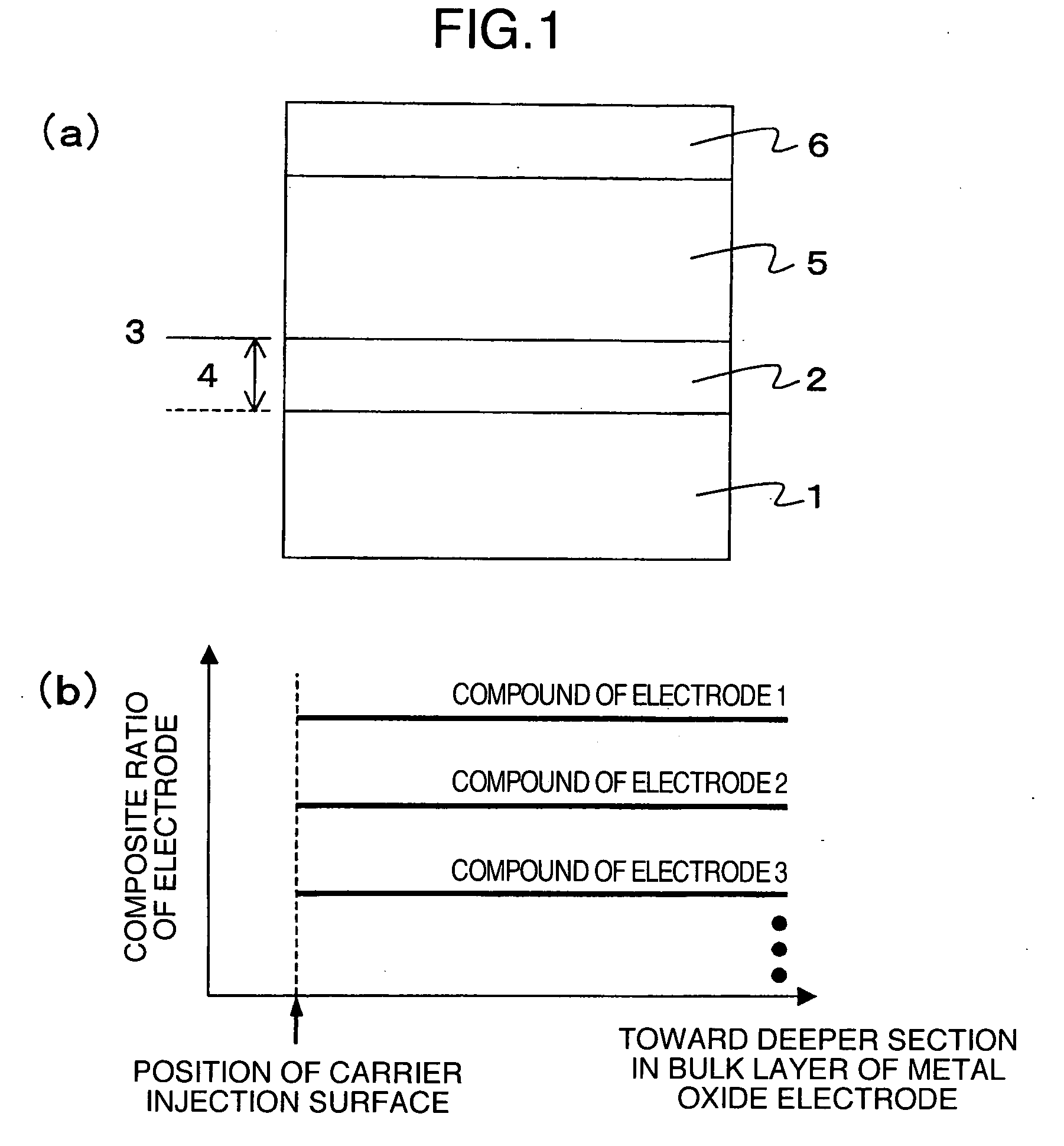
[0266] In Table 4, metal oxide electrodes having various composite distributions are provided by combining metal oxide electrodes and surface treatment types as desired. The composite ratios are substantially uniform when the sputter time is long, that is, in a deeper section in the bulk layer of the metal oxide electrode....


PUM


Abstract

An organic electroluminescence device is provided which employs a metal oxide electrode having particular composition distribution of elements to extend the life. A conventional approach for extending the life of an electroluminescence device is not provided by considering the degradation mechanism of how the organic electroluminescence device is degraded by the driving with electric current. The composite ratio of compounds of an electrode made of metal oxide forming part of the organic electroluminescence device is substantially uniform from a surface through which the carriers are injected from the electrode toward a deeper section in a bulk layer of the electrode. Thus, the electrode has stoichiometrically stable composition to prevent the degradation of electrode materials and diffusion into the organic layer, thereby providing a longer life.

Description

FIELD OF THE INVENTION [0001] The present invention relates to an organic electroluminescence device and an organic electroluminescence system, and more particularly, to an organic electroluminescence device with a thin film, a light weight, high definition, high efficiency, and a long life, preferable for use in a flat panel display, a small-size portable projection display, a display panel in a cellular phone, a three-dimensional display, an electric paper, a display in a portable personal computer, a real-time electronic signboard. BACKGROUND OF THE INVENTION [0002] In recent years, the widespread use of various types of cellular phones, mobile terminals, mobile computers, and car navigators has increased demands for lightweight, high-definition, high-brightness, and inexpensive small-size flat panel displays. [0003] In households and offices, small-footprint desktop displays and flat panel displays such as wall-mounted televisions are replacing conventional CRT displays. [0004] ...

Claims


Application Information

Patent Timeline
IPC IPC(8): H05B33/14H01L51/50
CPCH01L51/5206H10K59/17H10K50/81
Inventor IMANISHI, YASUO
Owner SAMSUNG DISPLAY CO LTD
Why Eureka
Try Eureka