
Single-VCO CDR for TMDS data at gigabit rate

a tmds data and synchronization clock technology, applied in the field of circuits and systems for the recovery and regeneration of data and synchronizing clock signals, can solve problems such as deterioration of phase quantization errors in approaches, increased design complexity, and errors during over-sampling, and achieve better jitter tolerance

Inactive Publication Date: 2006-11-16
KARMIC DESIGN USA
View PDF8 Cites 48 Cited by
  • Summary
  • Abstract
  • Description
  • Claims
  • Application Information

AI Technical Summary

Benefits of technology

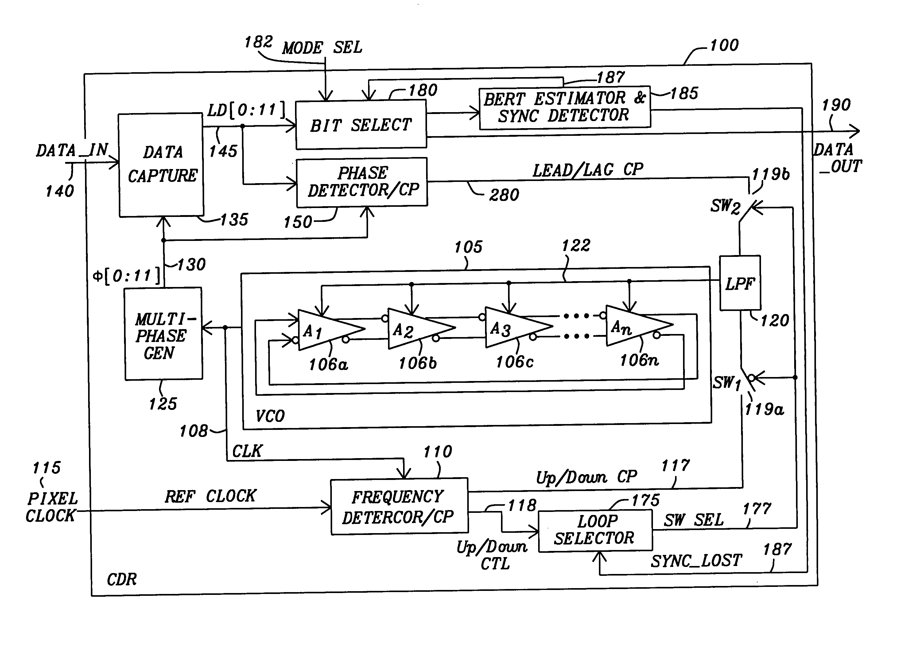
"This patent describes a communication system with a clock and data recovery circuit that can recover transmitted data and a synchronizing clock, even when the clock varies widely over a frequency spectrum. The circuit uses a voltage controlled oscillator to track the data and a multiple phase generator to create multiple phased clocking signals. A phase detector and low pass filter are used to determine if the clock is in phase with the data. The recovered data is then selected for further processing based on its bit error rate. The system also includes a bit error estimator and synchronization detector to ensure the data is synchronized with the reference clock. The technical effects of this invention include improved data recovery and synchronization, as well as better jitter tolerance and bit error control."

Problems solved by technology

This approach exhibits deteriorated phase quantization error due to the increased phase interval.
Therefore careful correction is necessary to remove the repeated bit or add the missing bit, which increases design complexity.
Besides, as the clocks and data don't necessarily remain synchronized, error may occur during the over-sampling due to metastability effect.
This may cause wrong decision for phase selection in DPLL and result in high bit error rate (BER).
Alternately, the over-sampling technique has a large phase quantization error that requires discrete adjustment.
Further the over-sampling as described above may cause the sampling faults requiring additional error correction complexity.
This added complexity contributes to a large power consumption of the circuits employing the over-sampling technique.
Error or jitter in edge spacing is introduced because of mismatch between the delay lines and their load capacitances.
This error or jitter requires large devices and careful layout.

Method used


Image

  • Single-VCO CDR for TMDS data at gigabit rate
  • Single-VCO CDR for TMDS data at gigabit rate
  • Single-VCO CDR for TMDS data at gigabit rate

Examples


Embodiment Construction

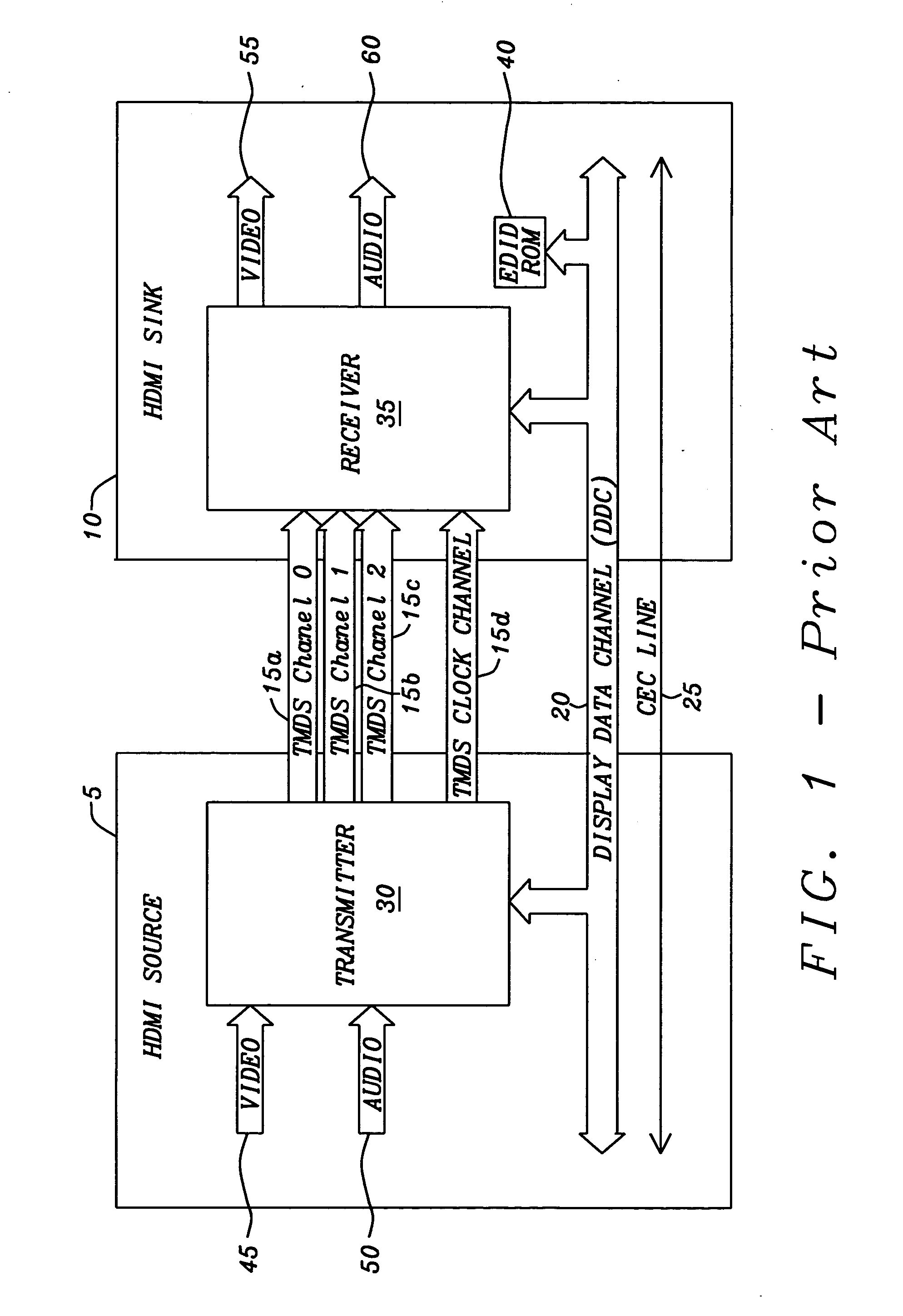
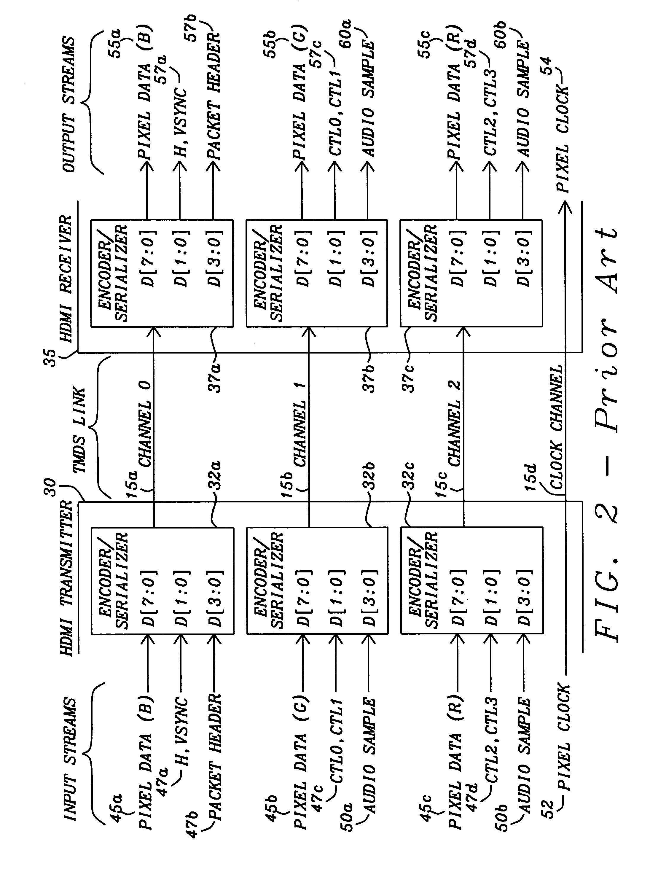
[0043] In communications systems such as the Transition Minimized Differential Signaling (TMDS) data and clock channels of the HDMI™, there is a need for clock and data recovery circuits that provide simplicity, low power consumption and small area, while having the ability to operate over a broad range of frequencies. The HDMl™ has a transmission data rate that varies from 250 Mbps to 1.65 Gbps. The communication system of this invention includes a clock and data recovery system that has a single voltage controlled oscillator (VCO) to synchronize the TMDS data using a binary (bang-bang) phase detector. The VCO is a ring oscillator having serially connected cross coupled differential amplifiers. Each of the amplifiers has their output cross connected to the inputs of the following differential amplifier. The last differential amplifier is in turned connected to the inputs of the first differential amplifier. The differential amplifiers each have a biasing connection to adjust the de...


PUM


Abstract

A clock and data recovery circuit has a voltage controlled oscillator that provides a clocking signal synchronized to a received serialized data. A multiple phase generator converts the clocking signal to a plurality of multiple phased clocking signals. A data capture device acquires the serialized data with each of the plurality of multiple phased clocking signals to create multiple phased data signals. A phase detector determines if the clocking signal is in phase with the recovered serialized data and providing a lead signal and a lag signal indicating whether the clocking signal is in phase with the recovered serialized data. A frequency initializing device assists acquisition of lock of the voltage controlled oscillator to a reference clock signal. A recovered data selector selects which of the multiple phased data signals are to be transferred to external circuitry for further processing.

Description

BACKGROUND OF THE INVENTION [0001] 1. Field of the Invention [0002] This invention relates generally to a circuits and systems for the recovery and regeneration of data and synchronizing clock signals received from a serial transmission channel. More particularly this invention relates to circuits and systems for recovery and regeneration of data and synchronizing clock signals while overcoming skew and jitter within the transmitted data and clock signals. [0003] 2. Description of Related Art [0004] As commercial and cable television has migrated to high definition digital transmission, equipment manufacturers have cooperated to create the specifications such as the High-Definition Multimedia Interface (HDMI™) developed by Hitachi, Ltd., Matsushita Electric Industrial Co., Ltd., Philips Consumer Electronics, International B.V., Silicon Image, Inc., Sony Corporation, and Thomson Inc. [0005] Toshiba Corporation, and the digital visual interface (DVI) specification, as promulgated by t...

Claims


Application Information

Patent Timeline
Patent Type & Authority Applications(United States)
IPC IPC(8): H03D3/24
CPCH03D13/004H04L7/0004H04L7/0012H04L7/033H04L7/046
Inventor ON, AUYONG, DINGSINGH, RAJINDER
Owner KARMIC DESIGN USA
Learn More