
Semiconductor device and manufacturing method thereof

a semiconductor device and semiconductor technology, applied in semiconductor devices, capacitors, electrical devices, etc., can solve the problems of ferroelectric capacitor damage, ferroelectric capacitor quality degradation, and difficulty in manufacturing a high-quality semiconductor device having a ferroelectric, so as to prevent the deterioration of the ferroelectric capacitor and increase the etching efficiency at the time of forming contact wiring

Inactive Publication Date: 2006-11-23
FUJITSU SEMICON LTD
View PDF13 Cites 17 Cited by
  • Summary
  • Abstract
  • Description
  • Claims
  • Application Information

AI Technical Summary

Benefits of technology

"The present invention provides a semiconductor device with a high-quality ferroelectric capacitor that is prevented from damage caused by the diffusion of hydrogen or H2O. The invention also includes a manufacturing method that increases the yield and efficiency of the semiconductor device while preventing deterioration of the ferroelectric capacitor. Additionally, the invention provides a low temperature aerosol cleaning method that removes particles while preventing deterioration of the ferroelectric capacitor. Overall, the invention provides a solution for preventing damage to the ferroelectric capacitor and improving the manufacturing efficiency of semiconductor devices."

Problems solved by technology

However, it is known that quality of the ferroelectric capacitor is degraded by hydrogen and water.
Therefore, since the reduction of the quality of the ferroelectric capacitor must be prevented by preventing the diffusion of hydrogen and water, there is difficulty in manufacturing a high-quality semiconductor device having a ferroelectric capacitor (in some cases, hereinafter referred to as FeRAM).
However, in a case where Cu is used as the wiring material, in some cases, the ferroelectric capacitor is damaged by the diffusion of hydrogen when the wiring structure is being formed.
In this case, the ferroelectric capacitor is damaged by processes including hydrogen diffusion generated at the time of forming the SiN film.
However, when the scrubber process is executed in the manufacturing process of the FeRAM, there is a risk that H2O will be diffused and the ferroelectric capacity will be damaged, and further, it is difficult to execute the scrubber process after forming the ferroelectric capacitor.
Consequently, in the manufacturing process of the FeRAM, it is difficult to increase the yield by removing the particles while preventing the deterioration of the ferroelectric capacitor caused by H2O.
Consequently, the efficiency at the time of forming the contact wiring of the ferroelectric capacitor becomes worse.

Method used


Image

  • Semiconductor device and manufacturing method thereof
  • Semiconductor device and manufacturing method thereof
  • Semiconductor device and manufacturing method thereof

Examples


first embodiment

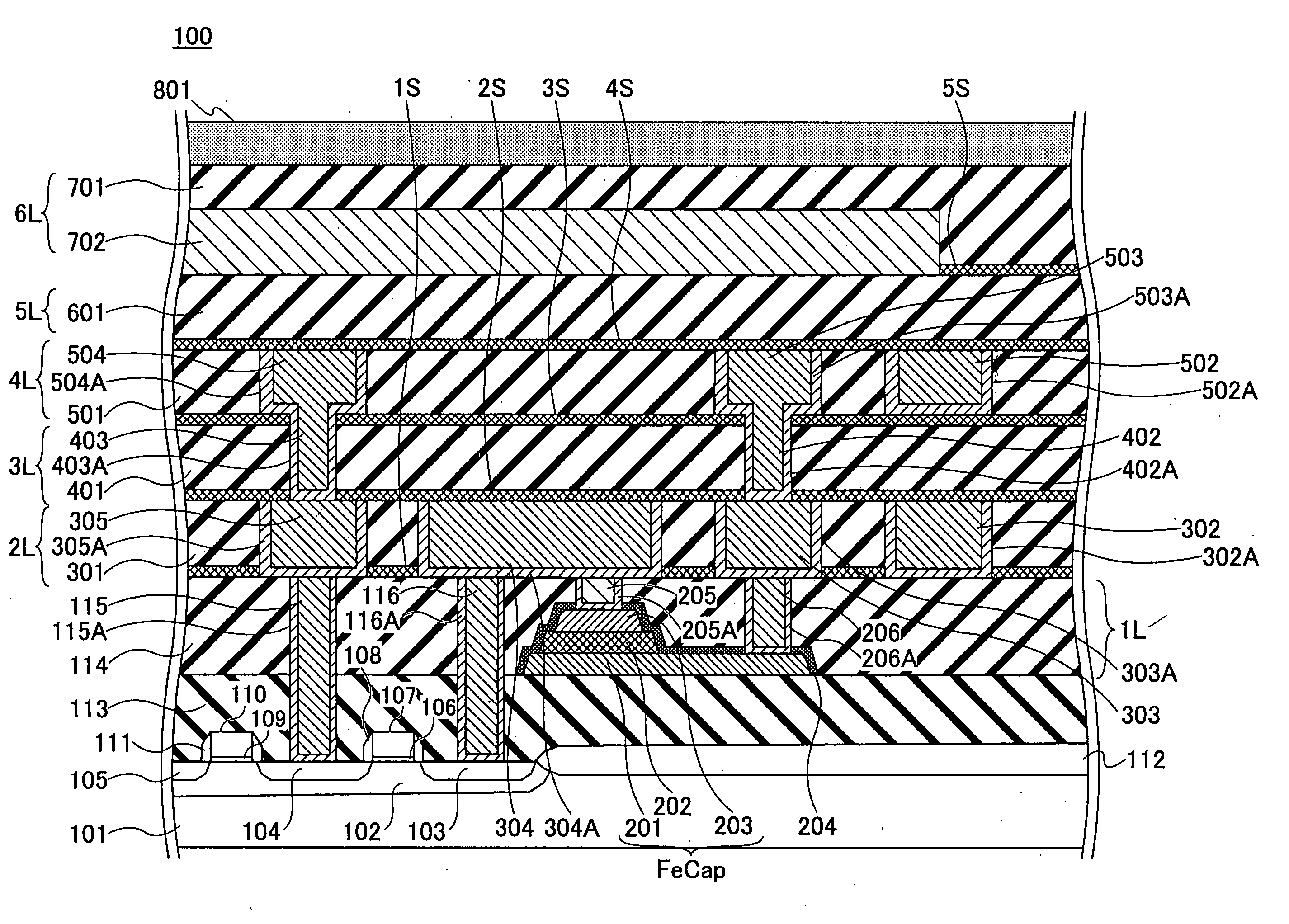
[0042]FIG. 1 is a schematic cross-sectional view of a semiconductor device 100 which has a ferroelectric capacitor according to a first embodiment of the present invention.

[0043] As shown in FIG. 1, the semiconductor device 100 has a ferroelectric capacitor that is formed on a layer in which layer a transistor and so on are formed on a silicon substrate 101, and a multi-layer wiring structure is formed on the ferroelectric capacitor.

[0044] The transistor is formed in an element region isolated by an element isolation insulating layer 112 on the silicon substrate 101. In the element region, an impurity diffusion layer 102 is formed to surround impurity diffusion layers 103, 104, and 105.

[0045] A gate insulation layer 106 is formed on the silicon substrate 101 sandwiched between the impurity diffusion layers 103 and 104. A gate electrode 107 is formed on the gate insulation layer 106, and a side wall insulation layer 108 is formed on the side wall of the gate electrode 107. With th...

second embodiment

[0142] When a hydrogen diffusion preventing layer is used as an etching stopper layer, it is desirable that etching selectivity with the dielectric inter layer be high. However, when the hydrogen diffusion preventing layer is not used as the etching stopper layer, since the etching selectivity with the dielectric inter layer is high, in some cases, the etching efficiency becomes worse.

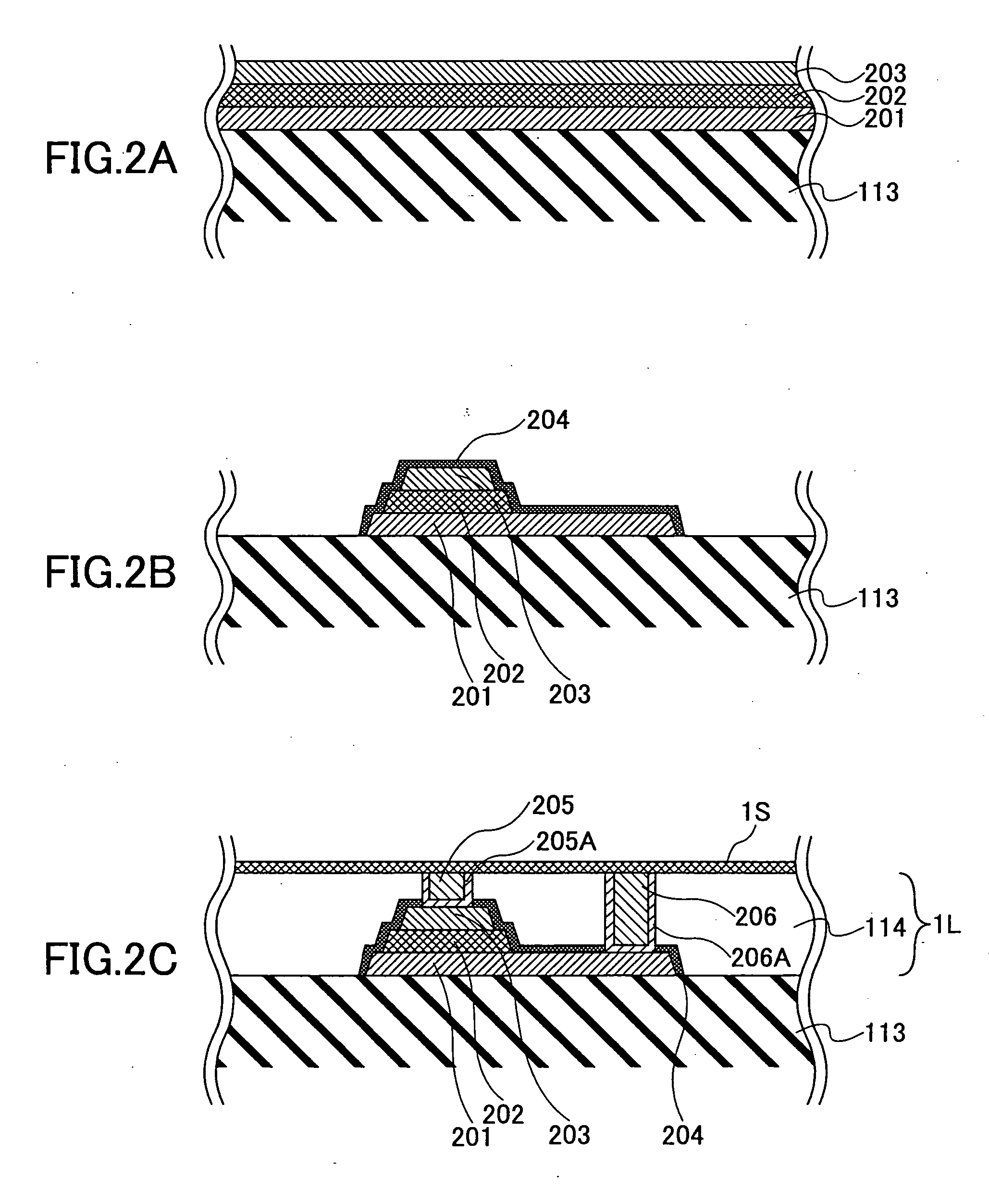
[0143] For example, as shown in FIG. 2C, in case of the hydrogen diffusion preventing layer 204 into which the contact wirings 205 and 206 of the ferroelectric capacitor are inserted, when the contact wirings 205 and 206 are formed by etching the dielectric inter layer 114 and the hydrogen diffusion preventing layer 204, at the time of etching, an etching gas and the etching conditions must be different between etching the dielectric inter layer 114 and etching the hydrogen diffusion preventing layer 204. Consequently, the etching efficiency at the time of forming the contact holes becomes worse.

[014...


PUM


Abstract

A semiconductor device is disclosed. The semiconductor device includes a ferroelectric capacitor formed on a substrate and a wiring structure formed on the ferroelectric capacitor. The wiring structure includes a dielectric inter layer and a Cu wiring section formed in the dielectric inter layer. In addition, an etching stopper layer including a hydrogen diffusion preventing layer is formed so as to face the dielectric inter layer.

Description

CROSS-REFERENCE TO RELATED APPLICATION [0001] This application is a U.S. continuation application filed under 35 USC 111(a) claiming benefit under 35 USC 120 and 365(c) of PCT application JP2003 / 016986, filed Dec. 26, 2003. The foregoing application is hereby incorporated herein by reference.BACKGROUND OF THE INVENTION [0002] 1. Field of the Invention [0003] The present invention generally relates to a semiconductor device having a ferroelectric capacitor and a manufacturing method thereof. [0004] 2. Description of the Related Art [0005] Recently, as a non-volatile memory which operates at highspeed and low power, a ferroelectric memory using a ferroelectric capacitor has been taken notice of and research and development of it has been greatly expanded. [0006] For example, in the ferroelectric capacitor, a ferroelectric material having a perovskite crystal structure is used. That is, PZT (Pb(Zr, Ti)O3), SBT (SrBi2Ta2O9), and so on is used. [0007] However, it is known that quality of...

Claims


Application Information

Patent Timeline
Patent Type & Authority Applications(United States)
IPC IPC(8): H01L29/94H01L21/02H01L27/10H01L27/105
CPCH01L28/57
Inventor IZUMI, KAZUTOSHI
Owner FUJITSU SEMICON LTD
Learn More