Semiconductor photodetector and method for manufacturing the same

a technology of semiconductors and photodetectors, applied in the direction of semiconductor devices, basic electric elements, electrical appliances, etc., can solve the problems of insufficient multiplication factor, inability to achieve sufficient multiplication factor, inability to achieve sufficient multiplication factor, etc., and achieve the effect of enhancing reliability

Active Publication Date: 2006-12-07
SUMITOMO ELECTRIC DEVICE INNOVATIONS
View PDF8 Cites 53 Cited by
  • Summary
  • Abstract
  • Description
  • Claims
  • Application Information

AI Technical Summary

Benefits of technology

[0025] In the planar APD, an electric charge concentrates at the edge of the selective diffusion region and a breakdown occurs at a low voltage, therefore, a guard ring 63 is formed at the edge of the selective diffusion region as shown in FIG. 23. The guard ring 63 is formed by carrying out ion implantation of impurity (for example, Be) and by carrying out a heat treatment such that a gradual concentration gradient can be obtained. By forming such a guard ring 63, an electric charge is prevented from concentrating at the edge of the selective diffusion region and the electric field intensity that occurs at the pn junction is kept low and thus a breakdown is prevented from occurring at a low voltage.
[0026] The present invention has been developed while the above-mentioned problems being taken into consideration and an object thereof is to provide a semiconductor photodetector having a mesa structure such as a mesa APD, in which an edge breakdown is prevented from occurring and reliability can be enhanced, and a method for manufacturing the same.
[0032] Therefore, according to a semiconductor photodetector and a method for manufacturing the same, an advantage is obtained that an edge breakdown is prevented from occurring in a semiconductor photodetector having a mesa structure such as a mesa APD and reliability can be enhanced.

Problems solved by technology

If an edge breakdown occurs first, it is not possible to sufficiently raise the electric field intensity at the photodetective portion because the increase in voltage only causes current to flow.
Further, if an edge breakdown occurs at a voltage lower than the breakdown voltage at the photodetective portion, a sufficient multiplication factor cannot be obtained at the photodetective portion because the electric field intensity at the photodetective portion can not be raised sufficiently and sufficiently high photodetective sensitivity cannot be ensured, therefore, it is not possible to sufficiently function as an APD as a result.
Further, if an edge breakdown has occurred, excessive noises are caused to occur as a result, and this also raises a problem.

Method used


Image

  • Semiconductor photodetector and method for manufacturing the same
  • Semiconductor photodetector and method for manufacturing the same
  • Semiconductor photodetector and method for manufacturing the same

Examples


first embodiment

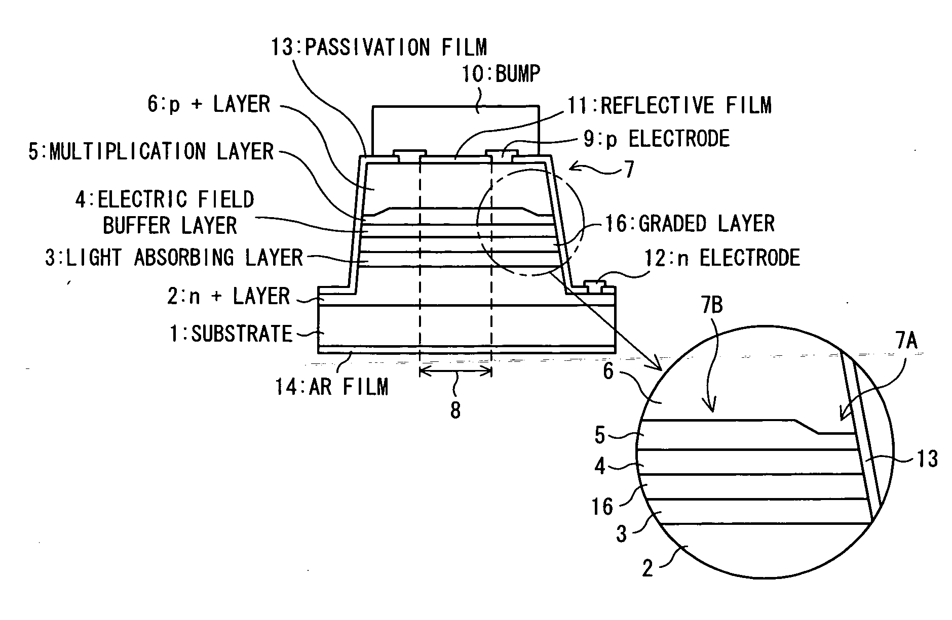
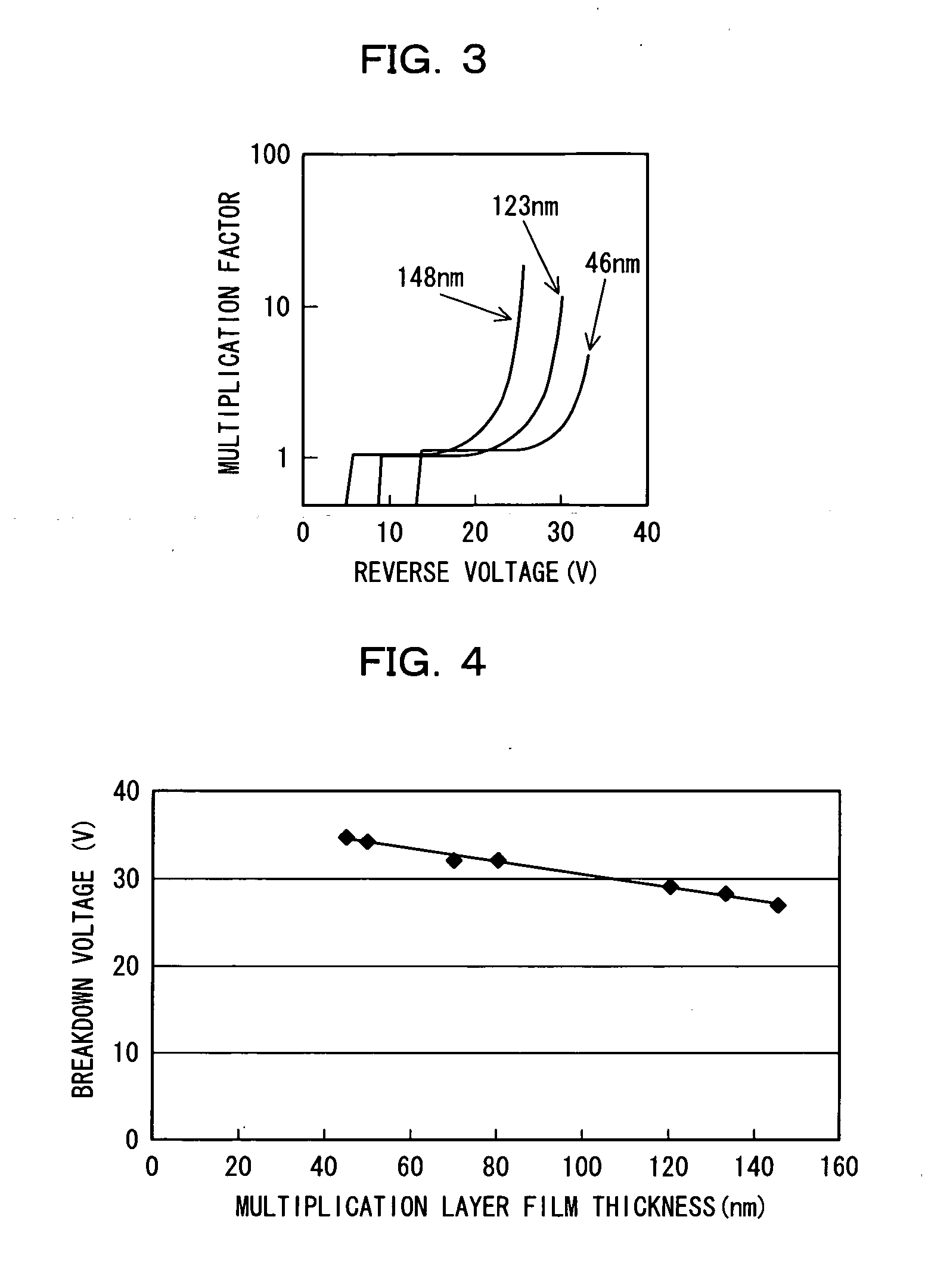
[0059] First, a semiconductor photodetector and a method for manufacturing the same according to a first embodiment of the present invention are described with reference to FIG. 1 to FIG. 6(B).

[0060] The semiconductor photodetector according to the present embodiment is, for example, an avalanche photodiode (APD), and is configured so as to comprise, as shown in FIG. 1, a mesa structure 7 in which at least an n+-InP buffer layer 2 (Si dope; concentration 1×1018 cm−3; n-type semiconductor layer; first semiconductor layer of the first conduction type), an i-InGaAs light absorbing layer 3 (undope; thickness 1 μm) for absorbing light, an i-InGaAsP graded layer 16 (graded composition layer, intermediate layer) for interpolating the discontinuity of the energy band between the light absorbing layer 3 and the avalanche multiplication layer 5, an n+-InP electric field buffer layer 4 (Si dope; concentration 1×1018 cm−3; thickness 0.05 μm; n-type semiconductor layer), an i-InP avalanche mult...

second embodiment

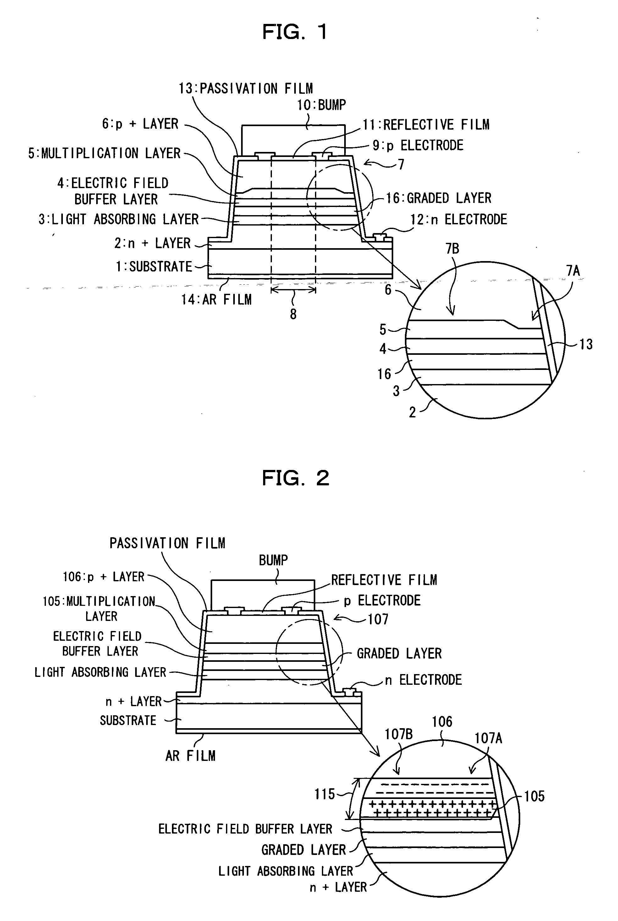
[0104] Next, a semiconductor photodetector and a method for manufacturing the same according to a second embodiment of the present invention are described below with reference to FIG. 8 and FIG. 9(A) to FIG. 9(D).

[0105] The semiconductor photodetector and its manufacturing method according to the present embodiment differ from those in the above-mentioned first embodiment in that the impurity concentration of the p-type semiconductor layer at the portion in the vicinity of the side face of the mesa structure is lower than the impurity concentration at the central portion. Since the manufacturing method is different, which will be described later, the configurations of the reflective film and the p-side electrode are different.

[0106] The semiconductor photodetector according to the present embodiment is, for example, an avalanche photodiode (APD) and is configured as the mesa structure 7 in which, as shown in FIG. 8, at least the n+-InP buffer layer 2 (n-type semiconductor layer; f...

third embodiment

[0135] Next, a semiconductor photodetector and a method for manufacturing the same according to a third embodiment of the present invention are described with reference to FIG. 10.

[0136] The semiconductor photodetector according to the present embodiment differs from the semiconductor photodetector in the above-mentioned first embodiment in that the passivation film has a two-layer structure.

[0137] As shown in FIG. 10, in the present semiconductor photodetector, an i-InP passivation film 30 (intrinsic semiconductor protective film, semiconductor passivation film) is formed at the side face of the mesa structure 7 (the concentration distribution is the same as that in the above-mentioned first embodiment) formed by, for example, growth junction and the surface of the buffer layer 2, and further, an SiN passivation film (insulating protective film, insulator passivation film) 31 is formed so as to cover the entire surface [the top surface of the i-InP passivation film 30 and the mes...


PUM


Abstract

In order to improve reliability by preventing an edge breakdown in a semiconductor photodetector having a mesa structure such as a mesa APD, the semiconductor photodetector comprises a mesa structure formed on a first semiconductor layer of the first conduction type formed on a semiconductor substrate, the mesa structure including a light absorbing layer for absorbing light, an electric field buffer layer for dropping an electric field intensity, an avalanche multiplication layer for causing avalanche multiplication to occur, and a second semiconductor layer of the second conduction type, wherein the thickness of the avalanche multiplication layer at the portion in the vicinity of the side face of the mesa structure is made thinner than the thickness at the central portion of the mesa structure.

Description

CROSS REFERENCE TO RELATED APPLICATIONS [0001] This application is based on and hereby claims priority to Japanese Application No. 2005-162416 filed on filed on Jun. 2, 2005 in Japan, the contents of which are hereby incorporated by reference. BACKGROUND OF THE INVENTION [0002] (1) Field of the Invention [0003] The present invention relates to a semiconductor device used in, for example, an optical communication system and, more particularly, to a semiconductor photodetector and a method for manufacturing the same, suitable for use as an avalanche photo diode (APD) having a mesa structure advantageous in reducing capacitance. [0004] (2) Description of Related Art [0005] Recently, following a considerable increase in demand for communication due to the prevalence of the Internet, a higher-speed optical communication system is demanded. For example, a photodetective device used in an optical communication system is required to provide a data transmission rate equal to or greater than ...

Claims


Application Information

Patent Timeline
Patent Type & Authority Applications(United States)
IPC IPC(8): H01L31/107
CPCH01L31/0232H01L31/107H01L31/1864H01L31/1075H01L31/035281H01L31/02327
Inventor YASUOKA, NAMIKUWATSUKA, HARUHIKOUCHIDA, TORUYONEDA, YOSHIHIRO
Owner SUMITOMO ELECTRIC DEVICE INNOVATIONS
Why Eureka
Try Eureka