Switching power supply device

a technology of switching power supply and control circuit, which is applied in the direction of electric variable regulation, instruments, manufacturing tools, etc., can solve the problems of unstable operation of the control circuit on-time control of the high-side switching device, and further reduction of power consumption, so as to reduce power consumption and device size, and increase efficiency

Inactive Publication Date: 2006-12-07
COLLABO INNOVATIONS INC
View PDF2 Cites 14 Cited by
  • Summary
  • Abstract
  • Description
  • Claims
  • Application Information

AI Technical Summary

Benefits of technology

[0034] The present invention is directed to solving these problems, and an object of the invention is to further increase efficiency and reduce power consumption and device size in a switching power supply.

Problems solved by technology

As a result, on-time control of the high-side switching device is extremely difficult when the high-side switching device is on because the supply voltage of the high-side switching device control circuit discharges naturally and gradually drops.
More specifically, this renders operation of the high-side switching device control circuit unstable.
(1) The peak level of current flowing to the switching device drops in the no-load state with PWM control of the step-down voltage switching power supply taught in the third example of the prior art above, but further reduction in power consumption is difficult because the number of switching operations is constant irrespective of the load.
(3) With the voltage step-down power supply device described in the first and second examples of the prior art, the high-side switching devices are switched on / off by the voltage at both ends of the capacitors in the bootstrap circuit, and a loss of control precision caused by the drop in capacitor voltage and fluctuation in the drain current caused by the fluctuating gate voltage of the switching device both occur easily.
(4) The input voltage range of the voltage step-down power supply device described in the first and second examples of the prior art is limited because use only at a relatively low voltage is difficult.
This increases power loss in the diodes during steady state operation, and thus prevents further improvement in power efficiency.

Method used


Image

  • Switching power supply device
  • Switching power supply device
  • Switching power supply device

Examples


embodiment 1

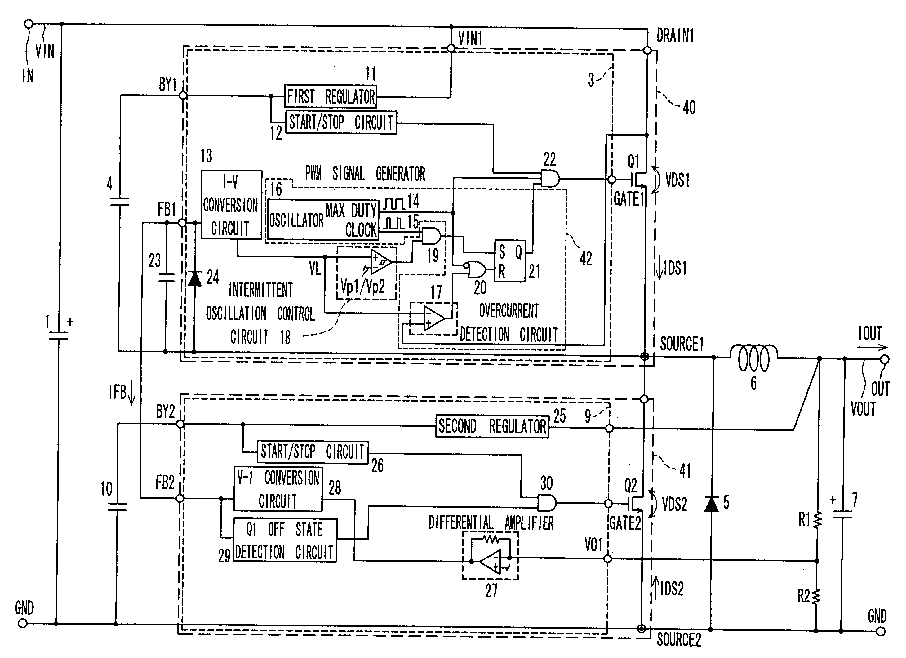
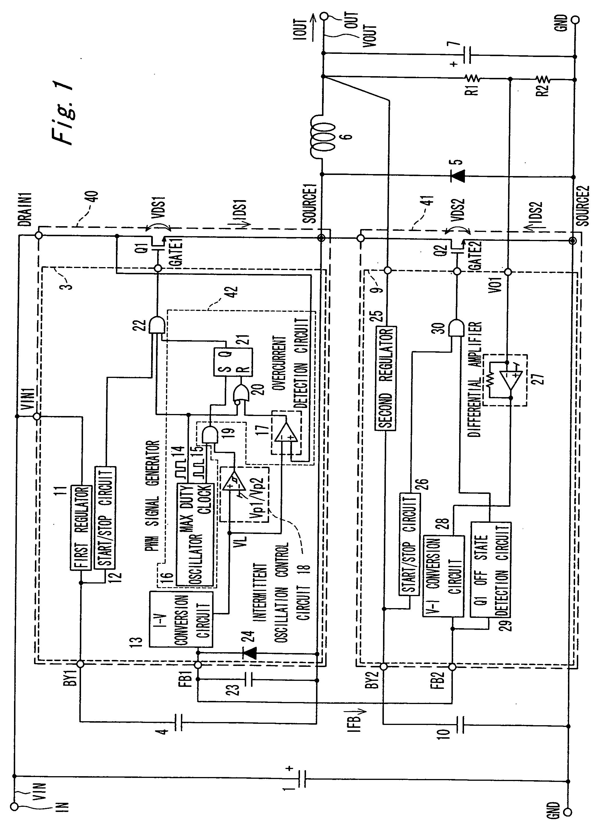
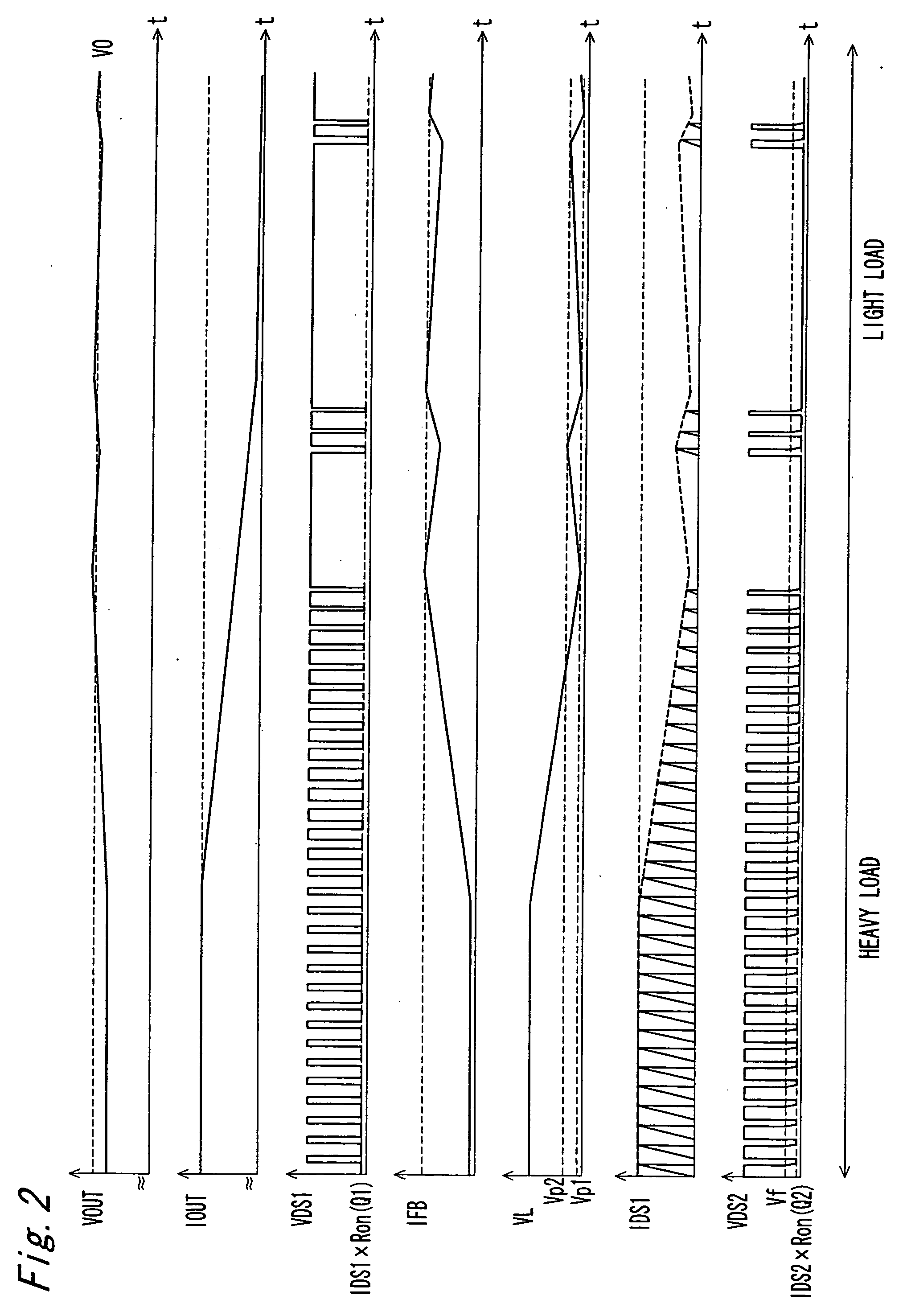
[0053]FIG. 1 shows a switching power supply device according to a first embodiment of the invention, and FIG. 2 shows the operating waves when the output load of the switching power supply in this first embodiment of the invention changes from a heavy load to a light load. In FIG. 1 and FIG. 2 the first supply voltage VIN is the voltage input to the input terminal IN from the first power supply voltage supply device where the ground potential of the ground terminal GND is the lowest potential; the second supply voltage VOUT is the voltage output from output terminal OUT where the lowest potential is the ground potential; IOUT is the current level at output terminal OUT; VDS1 is the DRAIN1 voltage of switching device Q1; IFB is the FB1 node current (=FB2 node current); IDS1 is the DRAIN1 current flowing through switching device Q1.

[0054] The switching power supply device according to this first embodiment of the invention comprises input capacitor 1, switching device Q1 and switchin...

second embodiment

[0075]FIG. 3 shows a switching power supply device according to a second embodiment of the invention. This embodiment of the invention renders a negative output power supply by connecting the negative terminal of the input capacitor 1 connected to the anode of the third diode 5 in FIG. 1 to the positive terminal of the output capacitor 7. As a result, the minimum potential of the second supply voltage VOUT is equal to the minimum potential of the first supply voltage VIN minus second supply voltage VOUT.

[0076] More specifically, the polarity of the second supply voltage is the same as the polarity of the first supply voltage in the first embodiment of the invention shown in FIG. 1, but in the second embodiment of the invention shown in FIG. 3 the polarity of the second supply voltage is the opposite of the polarity of the first supply voltage. The power supply operation is the same as in the switching power supply device of the first embodiment of the invention.

[0077] In addition ...

third embodiment

[0078]FIG. 4 shows a switching power supply device according to a third embodiment of the invention. In this embodiment of the invention power is supplied to the second regulator 25 of the control circuit 9 not from second supply voltage VOUT but instead directly from first supply voltage VIN. The power supply operation is the same as in the switching power supply device of the first embodiment of the invention.

[0079] In addition to the effects afforded by the first embodiment of the invention, using a switching power supply device according to this third embodiment of the invention enables easily lowering the output voltage.


PUM

PropertyMeasurementUnit
input supply voltageaaaaaaaaaa
voltageaaaaaaaaaa
currentaaaaaaaaaa

Abstract

The peak current flowing to the switching device drops in a no-load state with PWM control, but because the number of switching operations is constant regardless of the load, further reducing power consumption is difficult. The switching power supply device has a PWM signal generator for generating a PWM signal, a switching device Q1 for switching the first supply voltage VIN based on the PWM signal, converters for outputting the difference between a second supply voltage and a reference voltage as a difference signal, and an intermittent oscillation control circuit for stopping the switching operation of the first switching device when the difference signal is less than a predetermined first threshold value (Vp1). The PWM signal generator changes the pulse width based on the difference signal to generate the PWM signal.

Description

BACKGROUND OF THE INVENTION [0001] 1. Field of Technology [0002] The present invention relates to a switching power supply device, and relates more particularly to an apparatus that enables power conservation during standby mode operation and high efficiency during operation at a rated load. [0003] 2. Description of Related Art [0004]FIG. 9, FIG. 10, and FIG. 11 show examples of a step-down voltage type switching power supply. Step-down voltage switching power supplies include power supply devices with a bootstrap circuit to assure control power for the high side block as shown in FIG. 9 and FIG. 10, and power supply devices that do not have a bootstrap circuit and control the switching power using only the high side block as shown in FIG. 11. [0005]FIG. 9 shows a first example of the prior art described in Japanese Unexamined Patent Appl. Pub. 2000-350440. Operation of the control circuit 108 in the first example of the prior art shown in FIG. 9 is referenced to the ground terminal...

Claims


Application Information

Patent Timeline
Patent Type & Authority Applications(United States)
IPC IPC(8): B23K11/24
CPCB23K9/1056
Inventor HACHIYA, YOSHIAKIARAKAWA, RYUTAROFUKUI, MINORUKUNIMATSU, TAKASHI
Owner COLLABO INNOVATIONS INC
Why Eureka
Try Eureka