Method and apparatus for applying external coating to grid array packages for increased reliability and performance

a grid array and package technology, applied in the field of electrical circuit packaging, can solve the problems of limited extent of abrasive material removal of parylene coating from solder balls, and achieve the effects of improving mechanical containment of solder balls, improving electrical isolation, and improving processability of grid array packages

Inactive Publication Date: 2006-12-14
HONEYWELL INT INC
View PDF5 Cites 37 Cited by
  • Summary
  • Abstract
  • Description
  • Claims
  • Application Information

AI Technical Summary

Benefits of technology

[0007] The present invention provides a method and apparatus for selective removal of a conformal coating from the solder balls of grid array packages such that the benefits of the coating are realized. An ancillary benefit of the invention is improved process-ability of the grid array package by improving the mechanical containment of the solder during the reflow process and improved electrical isolation between the individual solder attachment points. In accordance with a preferred embodiment of the present invention, a method for coating a ball grid array is provided, which includes coating the entire external surface of the package with a thin layer of parylene. Next, the solder ball side of the part is butter smeared or squeegeed with a water soluble coating and assembled wet. A mask having holes in the same pattern as the balls in the grid, and a thickness that is about 80% of the height of the balls, is applied to the solder ball side of the part. This side of the part is then butter smeared again

Problems solved by technology

The extent that the abrasive material removes the parylene coating from the

Method used


Image

  • Method and apparatus for applying external coating to grid array packages for increased reliability and performance
  • Method and apparatus for applying external coating to grid array packages for increased reliability and performance
  • Method and apparatus for applying external coating to grid array packages for increased reliability and performance

Examples


Embodiment Construction

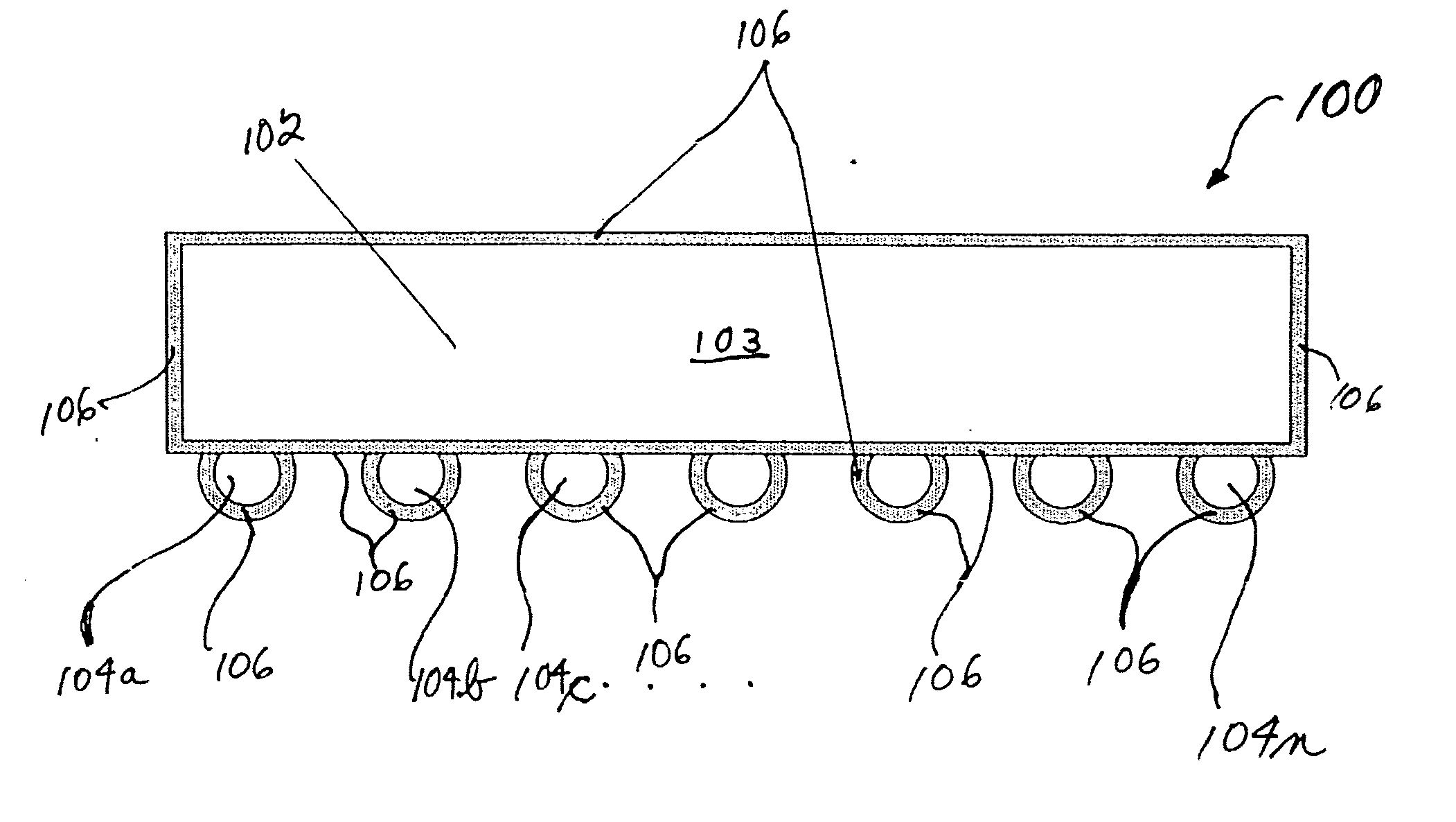
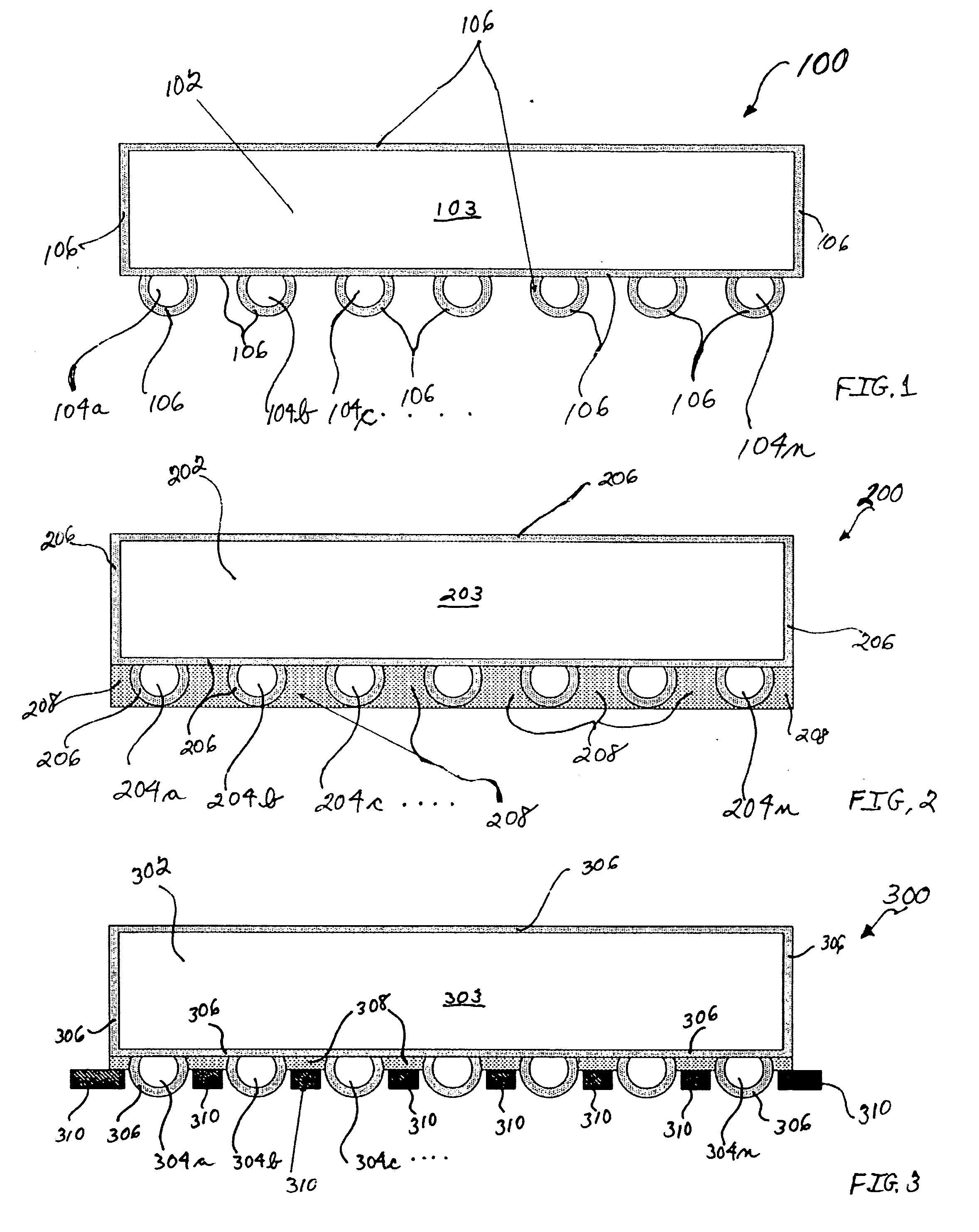
[0016] With reference now to the figures, FIG. 1 depicts a pictorial representation of a cut-away side view of an example surface mount package 100, which illustrates a method that can be used for coating a ball grid array in accordance with a preferred embodiment of the present invention. Notably, a surface mount package (100) including a plastic ball grid array package is shown in FIG. 1 for illustrative purposes, but the present invention is not intended to be so limited and can include within its scope other types of grid array packages (e.g., ceramic ball grid arrays, column ceramic ball grid arrays, flip-chip plastic ball grid arrays, etc.) or other surface mount packages, which can be coated with parylene or any other suitable material (e.g., other polymer material) having electrical and thermal properties similar to or as advantageous as parylene. For this example embodiment, surface mount package 100 includes a ball grid array package 102, an integrated circuit (denoted gen...


PUM


Abstract

A method and apparatus are disclosed for selective removal of a conformal coating from the solder balls of grid array packages such that the benefits of the coating are realized. An ancillary benefit of the invention is improved process-ability of the grid array package by improving the mechanical containment of the solder during the reflow process and improved electrical isolation between the individual solder attachment points. For example, a method for coating a ball grid array is provided, which includes coating the ball grid array with a thin layer of parylene. Next, the solder ball side of the part is butter smeared or squeegeed with a water soluble coating and assembled wet. A mask having holes in the same pattern as the balls in the grid, and a thickness that is about 80% of the height of the balls, is applied to the solder ball side of the part. This side of the part is then butter smeared again with the water soluble coating, and the entire assembly is allowed to dry. At this point, about 20% of each parylene-coated solder ball protrudes higher than the surface of the mask. The solder ball side of the part is then grit blasted with an abrasive material. The extent that the abrasive material removes the parylene coating from the solder balls is limited by the mask and the layer of water soluble coating. Therefore, the grit blasting removes the parylene coating from only the protruding areas (e.g., about top 20%) of the solder balls. Water is then used to remove the water soluble coating, and the parylene coated part is baked to remove moisture. Thus, a parylene coated ball grid array (or column grid array) is provided that is highly impervious to moisture, has a very high dielectric strength, and thereby improves the electrical performance and reliability of the surface mounted part.

Description

FIELD OF THE INVENTION [0001] The invention relates generally to the electronic circuit packaging field, and more specifically, but not exclusively, to a method and apparatus for increasing the reliability and performance of surface mount packages used for integrated circuits. More specifically, the invention relates to a method and apparatus for selective removal of a conformal coating from the solder balls of grid array packages such that the benefits of the coating are realized. An ancillary benefit of the invention is improved process-ability of the grid array package, by improving the mechanical containment of the solder during the reflow process and improved electrical isolation between the individual solder attachment points. BACKGROUND OF THE INVENTION [0002] A grid array package is a type of surface mount package used for integrated circuits. Two generic types of grid array packages are most common: ball grid arrays in which a small solder ball is used as the joining interf...

Claims


Application Information

Patent Timeline
IPC IPC(8): H01L23/053
CPCH01L21/4853H01L21/4864H01L23/3128H01L23/3135H05K3/3436H05K3/3457H01L2924/0002H05K2203/025H05K2203/0557H01L2924/00013H05K2201/0179H01L2224/13099H01L2224/13599H01L2224/05599H01L2224/05099H01L2224/29099H01L2224/29599H01L2924/00
Inventor BARNES, DAVID A.GROOMS, JASON C.MARTINEZ, NEAL B.MCKINNERNEY, JOSEPH M.
Owner HONEYWELL INT INC
Why Eureka
Try Eureka