Diamond-like carbon devices and methods for the use and manufacture thereof

Inactive Publication Date: 2006-12-21
SUNG CHIEN MIN
2 Cites 28 Cited by

AI-Extracted Technical Summary

Problems solved by technology

Although basically successful in many applications, thermionic devices have been less successful than field emission devices, as field emission devices generally achieve a higher current output.
Despite this key advantage, most field emission devices suffer from a variety of other shortcomings that limit their potential uses, including materials limitatio...

Method used

[0036] As used herein, “distorted tetrahedral coordination” refers to a tetrahedral bonding configuration of carbon atoms that is irregular, or has deviated from the normal tetrahedron configuration of diamond as described above. Such distortion generally results in lengthening of some bonds and shortening of others, as well as the variation of the bond angles between the bonds. Additionally, the distortion of the tetrahedron alters the characteristics and properties of the carbon to effectively lie between the characteristics of carbon bonded in sp3 configuration (i.e. diamond) and carbon bonded in sp2 configuration (i.e. graphite). One example of material having carbon atoms bonded in distorted tetrahedral bonding is amorphous diamond. A representation of carbon atoms bonded in distorted tetrahedral coordination is shown in FIG. 7. It will be understood that FIG. 7 is a representation of merely one possible distorted tetrahedral configuration and a wide variety of distorted configurations are generally present in amorphous diamond.
[0055] It has now been found that various diamond-like carbon materials can easily emit electrons when an energy source is applied. Such materials retain the NEA properties of diamond, but do not suffer from the band gap issues of pure diamond. Thus, electrons energized by applied energy are allowed to move readily through the diamond-like carbon material, and be emitted using significantly lower energy inputs, than those required by diamond. Further, the diamond-like carbon material of the present invention has been found to have a high energy absorption range, allowing for a wider range of energies to be converted into electrons, and thus increasing the conversion efficiency.
[0057] Another aspect of the present amorphous diamond material that facilitates electron emission is the presence of certain geometric configurations. Referring now to FIG. 1, is shown a side view of one embodiment of a configuration for the amorphous diamond material 5, made in accordance with the present invention. Specifically, the amorphous diamond material has an energy input surface 10, that receives energy, for example, thermal energy, and an emission surface 15 that emits electrons therefrom. In one aspect, in order to further facilitate the emission of electrons, the emission surface can be configured with an emission surface that has a roughness or asperity, that focuses electron flow and increases current output, such asperity represented here by a plurality of peaks or projections 20. It should be noted that although FIG. 1 illustrates uniform peaks, such is only for convenience, and that the amorphous diamond of the present invention is typically non-uniform and the distances between peaks and the peak heights can vary as shown in FIGS. 3 and 4.
[0061] In one aspect of the invention, the energy type utilized can be thermal energy. To this end, an energy absorber and collection layer can be used in connection with or coupled to the diamond-like carbon material of the present invention that aids in the absorption and transfer of heat into the material. As will be recognized by those of ordinary skill in the art, such an absorber can be composed of a variety of materials that are predisposed to the absorption of thermal energy, such as carbon black, etc. In accordance with the present invention, the thermal energy absorbed by the diamond-like carbon material can have a temperature of less than about 500° C. Additionally, the photonic or thermal energy can be sufficient to maintain the cathode at a temperature from about 100° C. to about 1800° C. Typically, an energy input of from about 200° C. to about 300° C. can be common. Additionally, absorber collection layers can be designed for absorbing photonic and/or thermal energy such as carbon black, sprayed graphite particles, or any other dark or black body. In one alternative, the absorber collection layer can have an increased surface roughness to enhance the amount of light and/or heat absorbed. Various methods of providing textured surfaces are known to those skilled in the art.
[0063] The diamond-like carbon material of the present invention can be further coupled to, or associated with a number of different components in order to create various devices. Referring now to FIG. 2, is shown one embodiment of a diamond-like carbon thermoelectric conversion device configured as an electrical generator in accordance with the present invention. Notably, the cathode 25 has a layer of diamond-like carbon material 5 coated thereon. The surface of the diamond-like carbon material which contacts the cathode is input surface 10. Further, as discussed above, an optional energy collection layer 40 can be coupled to the cathode opposite the diamond-like carbon layer. The energy collector can be included as desired, in order to enhance the collection and transmission of thermal or photonic energy to the diamond-like carbon material. An intermediate member 55 is electrically coupled to the electron emission surface 15 of the diamond-like carbon material 5. An anode 30 can be electrically coupled to the intermediate member opposite the diamond-like carbon material.
[0064] In an alternative embodiment, the diamond-like carbon material 5 can be coated on the anode 30, rather than the cathode 25. In some configurations, performance of the device can be improved by coating the anode with the diamond-like carbon. Alternatively, each of the anode and cathode can have diamond-like carbon coated thereon. It has been discovered that use of diamond-like carbon on the anode side can provide the desired electron emission, regardless of the presence of diamond-like carbon on the cathode emission surface. The presence of a diamond-like carbon layer on the anode appears to have a more significant affect on the electron emission than a diamond-like carbon layer on the cathode side. Thus, in some embodiments, the cathode can be in direct contact with the intermediate layer, e.g., without a diamond-like carbon layer, while the anode includes a layer of diamond-like carbon formed thereon. Typically, the asperities can be directed toward the intermediate layer. In this case the diamond-like carbon layer can be deposited on the anode as discussed herein with respect to the cathode. Alternatively, the diamond-like carbon layer can be formed on the intermediate layer such that the asperities are directed toward the anode. In this embodiment, the anode can then be formed on the diamond-like carbon layer via any suitable method such as those processes described above. Thus, all of the embodiments, materials, and configurations discussed elsewhere herein can be used in connection with devices which include diamond-like carbon on the anode.
[0067] In one aspect of the present invention, the entire diamond-like carbon thermoelectric conversion device is a solid assembly having each layer in continuous intimate contact with adjacent layers and/or members. Solid materials can often be more reliable, easier to manufacture, and can be more durable than those which require a vacuum or gas to be maintained. However, vacuum and gas intermediate members can also be suitable in some applications.
[0072] The base member 60 of the cathode 25 can be a single or multiple layers. In one embodiment, the base member is a single layer of material. In another embodiment, the base member includes a first layer and a second layer (not shown) such that the second layer is coupled between the first layer and the energy input surface of the amorphous diamond layer. The second layer acts to improve electron conduction to the emission surface of the diamond layer. Generally, when a second layer is used as part of the base member, it is preferred that the second layer comprise a material which has a work function which is less than the work function of the first layer. Typically, the second layer comprises a material having a low work function of from about 2.0 eV to about 4.0 eV, although work functions of from about 2.0 eV to about 3.0 eV are also suitable. More preferably, the second layer comprises a material having a work function of from about 1.5 eV to about 3.5 eV. Suitable materials for use in the second layer include, without limitation, Cs, Sm, Al—Mg, Li, Na, K, Rb, Be, Mg, Ca, Sr, Ba, B, Ce, Al, La, Eu, and mixtures or alloys thereof. In one specific aspect, the second layer can comprise Cs, Sm, Al—Mg and alloys thereof. In a more specific aspect, the second layer can comprise Be, Mg, Cs, or Sm, and most preferably Cs.
[0073] In order to improve heat transfer toward the diamond-like carbon layer, the second layer can comprise a material which has a thermal conductivity of greater than about 100 W/mK. As with other layers or members, a variety of thicknesses can be used however, the second layer is often from about 1 micron to about 1 millimeter. Those skilled in the art will recognize that typical low work function materials also readily oxidize. Thus, it may be desirable to form at least the second layer, and often the entire thermoelectric conversion device, under a vacuum or other inert environment.
[0074] Without wishing to be bound to any particular theory, the ability of the present invention to produce electricity can be viewed as a stepping process related to the band gap between materials, work function, and thermal conductivity of each layer. Specifically, the second layer of the cathode can be made of a material that acts to step the electrons closer to vacuum energy or conduction band, (i.e. decrease the band gap between the first layer and vacuum energy). Additionally, the second layer can have a high thermal conductivity in order to improve electron flow toward the electron emission surface. The electrons in the second layer can then be transmitted to the diamond-like carbon layer where the distorted tetrahedral coordinations of the amorphous diamond create a variety of different work function and band gap values (i.e. within the unoccupied conduction band) within the amorphous diamond layer, such that some of the electron states approach and exceed the vacuum energy.
[0075] The material for use in the intermediate member can then be chosen to minimize heat loss by allowing the electrons to transfer, or “step” back down to the anode material. This decreases the amount of energy which is lost in the system. For example, a large step from amorphous diamond down to a high work function material can be used in the present invention; however, some of the electrical energy is lost as heat. Thus, more than one intermediate member and/or base member l...

Benefits of technology

[0016] In some applications the intermediate material can be a solid material. Solid materials can often be more reliable, easier to manufacture, and can be more durable than those which require a vacuum or gas to be maintained. However, vacuum and fluid...

Abstract

Diamond-like carbon based devices and methods of making and using the same which have improved electron emission and increased reliability. The device can include an anode with a layer of diamond-like carbon material such as amorphous diamond coated over at least a portion of the anode and a cathode. An intermediate member can be electrically coupled between the diamond-like carbon material and the cathode. Various additional layers and configurations can allow for improved performance such as multiple cathode layers and/or multiple intermediate layers. The presence of diamond-like carbon on the anode provides significantly improved electron emission with or without diamond-like carbon on the cathode. The devices can be configured as thermoelectric conversion devices such as an electrical generator or a cooling device, light emitting devices, or other electronic devices and can be conveniently formed.

Application Domain

Thermionic cathodesDischarge tube main electrodes +3

Technology Topic

Amorphous diamondImproved performance +7

Image

  • Diamond-like carbon devices and methods for the use and manufacture thereof
  • Diamond-like carbon devices and methods for the use and manufacture thereof
  • Diamond-like carbon devices and methods for the use and manufacture thereof

Examples

  • Experimental program(15)

Example

EXAMPLE 1
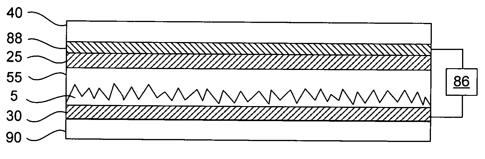
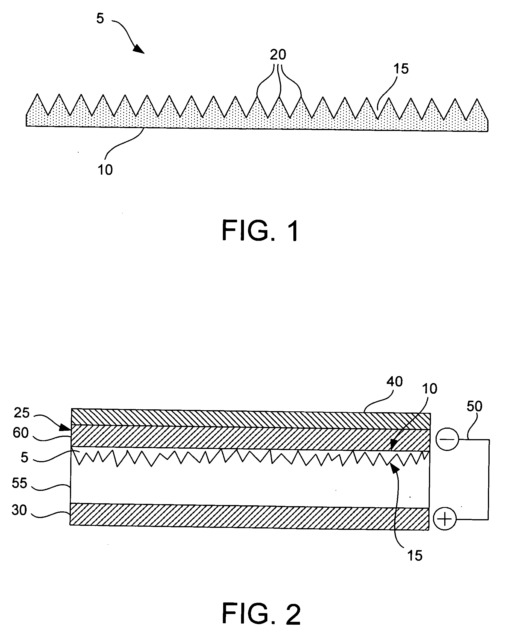
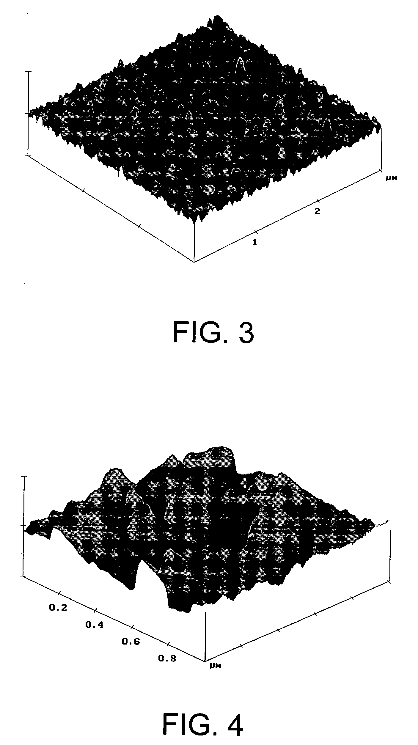
[0105] A copper foil is glued to a polyimide support layer. A one micron layer of amorphous diamond is deposited on the exposed copper foil electrode using a cathodic arc process. The amorphous diamond has a 50 nm asperity. An intermediate layer of PZT is deposited by screen printing to a thickness of 30 μm on the amorphous diamond. A layer of silver grease is coated on the PZT intermediate member by screen printing to form an anode. The assembly is then cured in an oven to drive off the binder used in screen printing and to consolidate the device. Attachment of wires to the copper electrodes can allow this thermoelectric conversion device to act as either an electrical generator by absorption of heat or as a cooling device by application of an electrical current.

Example

EXAMPLE 2
[0106] The same procedure is followed as in Example 1, except the PZT layer is replaced by a mixture of graphite powder and hexagonal boron nitride powder.

Example

EXAMPLE 3
[0107] The same procedure is followed as in Example 1, except the PZT layer is replaced by a mixture of graphite powder and aluminum oxide powder.

PUM

no PUM

Description & Claims & Application Information

We can also present the details of the Description, Claims and Application information to help users get a comprehensive understanding of the technical details of the patent, such as background art, summary of invention, brief description of drawings, description of embodiments, and other original content. On the other hand, users can also determine the specific scope of protection of the technology through the list of claims; as well as understand the changes in the life cycle of the technology with the presentation of the patent timeline. Login to view more.

Similar technology patents

Integrated cup insert jounce bumper

InactiveUS6158726AEasily manufactureCorrosion resistancePortable framesStands/trestlesCHEEK DIMPLESFastener
Owner:VIBRACOUSTIC NORTH AMERICA

Classification and recommendation of technical efficacy words

Why Eureka
Try Eureka