

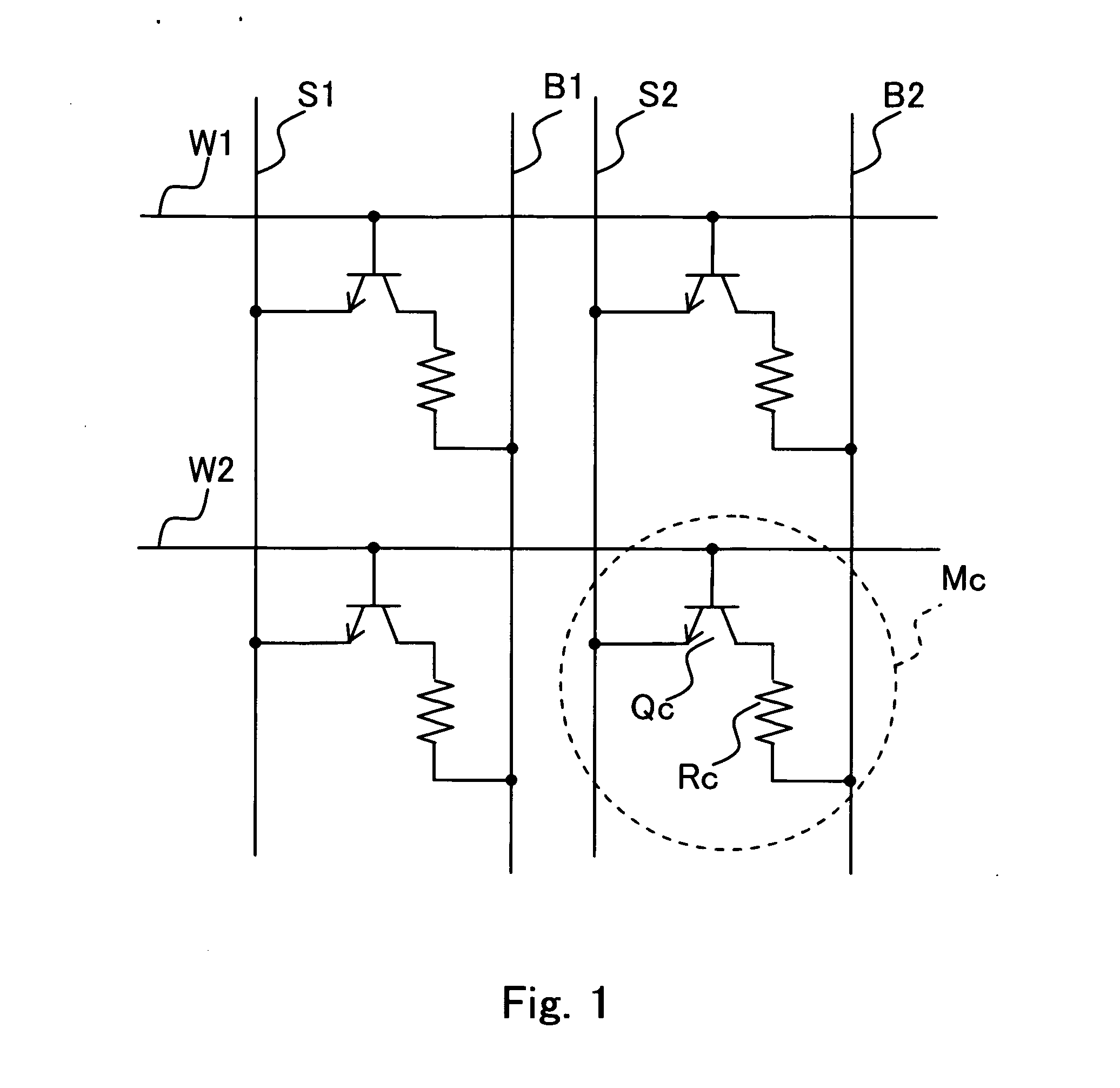
Memory cell, semiconductor memory device, and method of manufacturing the same
a memory device and semiconductor technology, applied in the field of memory devices, can solve the problems of inability to carry out writing, reading, resetting actions without the help of external signals, and the passage of current leakage between, so as to reduce the variation of characteristics, reduce manufacturing costs, and increase storage capacity of semiconductor memory devices.
- Summary
- Abstract
- Description
- Claims
- Application Information
AI Technical Summary
Benefits of technology
Problems solved by technology
Method used
Image

Examples
first embodiment
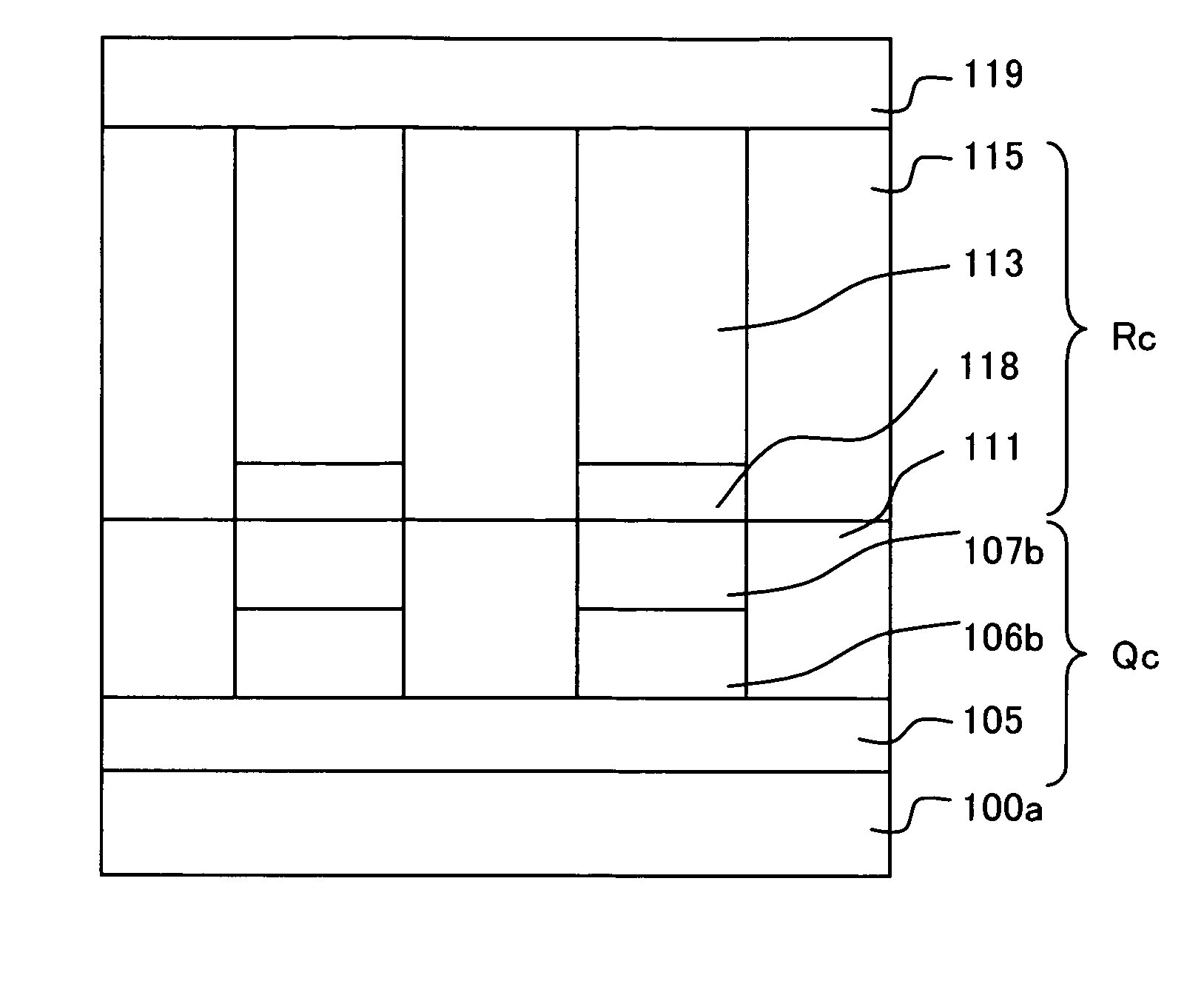
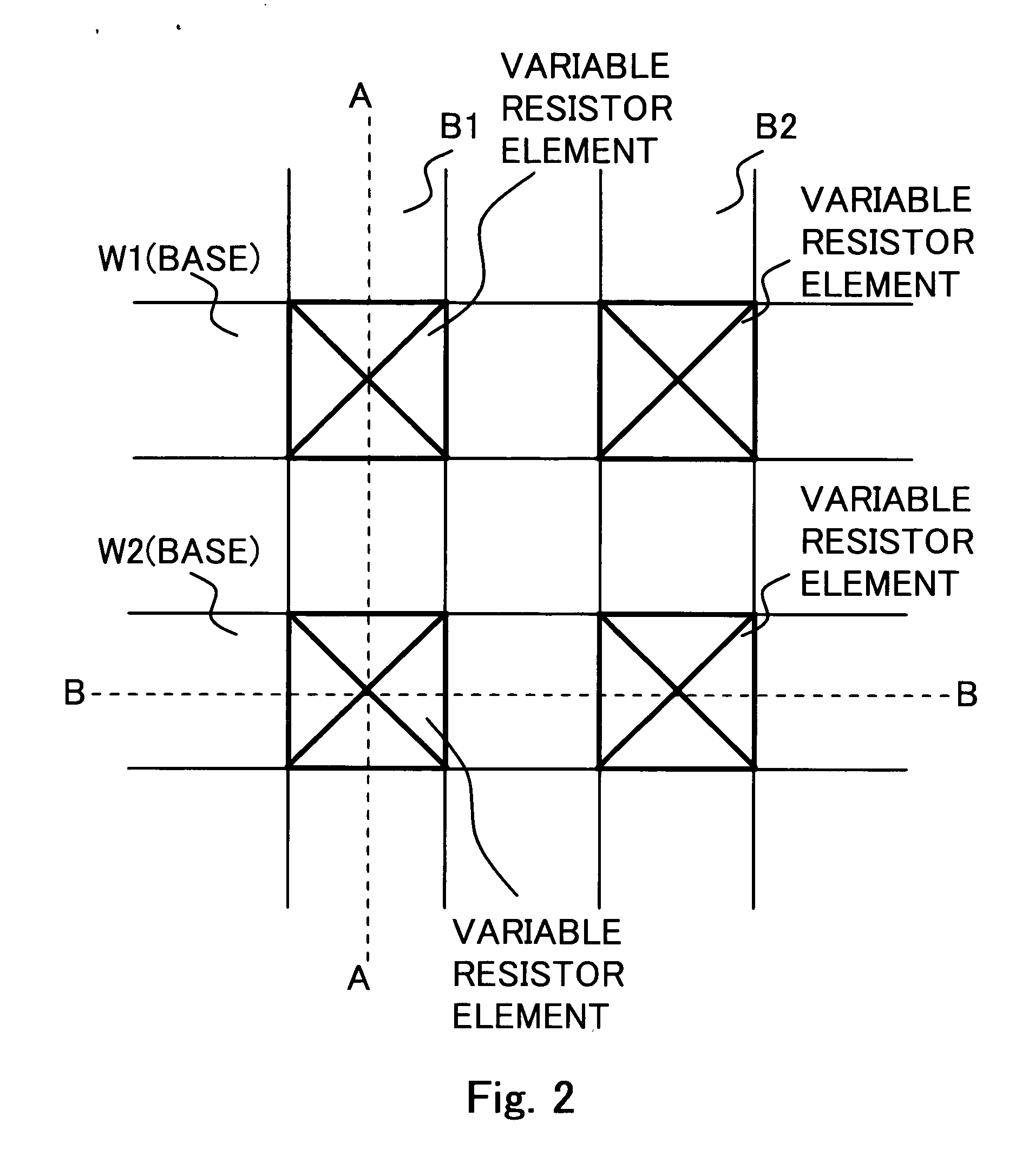
[0111] This embodiment will be described in the form of a semiconductor memory device where a second semiconductor layer and a third semiconductor layer are epitaxial silicon layers, referring to FIGS. 3 to 17. Each drawing denoted by the letter A represents a cross sectional view taken along the line A-A of a plan view of the memory array of FIG. 2 while each drawing denoted by the letter B is a cross sectional view taken along the line B-B of the same.
[0112] A silicon oxide layer 101 is deposited to a thickness of 10 to 100 nm as a mask layer on the surface of a p-type silicon substrate 100 which acts as the semiconductor substrate. Then, a silicon nitride layer 102 is deposited to a thickness of 50 to 500 nm. With a first resist mask 001 having been pattered over by a known photolithography manner (See FIG. 3), a reactive ion etching process is conducted to etch the silicon nitride layer 102 and the silicon oxide layer 101 in a sequence.
[0113] The p-type silicon substrate 100 i...
second embodiment
[0123] This embodiment will be described in the form of a semiconductor memory device where the second electrode and the variable resistor body are positioned by a self-alignment process in relation to the selected transistor, referring to FIGS. 18 to 29. Each drawing denoted by the letter A represents a cross sectional view taken along the line A-A of a plan view of the memory array of FIG. 2 while each drawing denoted by the letter B is a cross sectional view taken along the line B-B of the same. This embodiment is identical to the first embodiment up to the steps of filling the groove, which has been patterned using the resist mask 001, with an insulating layer or silicon oxide layer 103 (as shown in FIGS. 3 to 5).
[0124] After the silicon oxide layer 103 is developed in the groove, a p-type epitaxial silicon layer 104 is deposited to a thickness of 1 to 10 μm on the surface of the p-type silicon substrate 100a and the silicon oxide layer 103. It is desired that the p-type epitax...
third embodiment
[0133] This embodiment will be described in the form of a semiconductor memory device where a portion of the second semiconductor layer is a polycrystalline silicon layer, referring to FIGS. 34 to 37. Each drawing denoted by the letter A represents a cross sectional view taken along the line A-A of a plan view of the memory array of FIG. 2 while each drawing denoted by the letter B is a cross sectional view taken along the line B-B of the same. This embodiment is identical to the first embodiment up to the steps of filling the groove, which have been patterned using the resist mask 001, with an insulating layer or silicon oxide layer 103 (as shown in FIGS. 3 to 5).
[0134] After the silicon oxide layer 103 is developed in the groove, a polycrystalline silicon layer 109 is deposited to a thickness ranging from 100 nm to 5 μm on the surface of the p-type silicon substrate 100a and the silicon oxide layer 103 (See FIG. 34). Similarly, a p-type epitaxial silicon layer 110 is deposited to...
PUM
 Abstract
Description
Claims
Application Information