Eureka AIR delivers breakthrough ideas for toughest innovation challenges, trusted by R&D personnel around the world.

Method for operating a non-volatile charge-trapping memory device and method for determining programming/erase conditions

Inactive Publication Date: 2006-12-28
INTERUNIVERSITAIR MICRO ELECTRONICS CENT (IMEC VZW)
View PDF10 Cites 13 Cited by
  • Summary
  • Abstract
  • Description
  • Claims
  • Application Information

AI Technical Summary

Benefits of technology

[0009] With methods for determining programming and erase conditions as described herein, there should be substantially no change in the spatial charge distribution of the charge-trapping layer in programmed and erased states. The programming and erase conditions which are determined have to meet this requirement. As a result, there is no longer a need for adaptive cycling over the life of the device, since the threshold voltage window is maintained flat as a result of avoiding a change in the spatial charge distribution. Hence, the increase in the voltages can be avoided and power consumption can be reduced.
[0012] The above described method for determining the first, second and third spatial charge distributions has the advantage that not only the spatial charge distribution of charge stored the charge-trapping layer can be extracted, but also the spatial charge distribution of charge stored in interface traps. In this way, the spatial distribution of both electrons and holes in the dielectric layer can be obtained. The thus obtained hole and electron distribution profiles are used for physical understanding and optimisation of the programming and erase conditions. However, the first, second and third spatial charge distributions may also be determined in any other way known to the person skilled in the art.
[0015] According to this embodiment, programming and erase conditions are used for operating a non-volatile memory device, wherein there should be no change in the spatial charge distribution of the charge-trapping layer in programmed and erased states. As mentioned, this avoids the need for adaptive cycling over the life of the device, since the threshold voltage window is maintained flat as a result of avoiding a change in the spatial charge distribution. Hence, the increase in the voltages can be avoided and power consumption can be reduced.

Problems solved by technology

However, poor endurance and poor retention after cycling, i.e. repetitive programming and erasing of a cell, are major drawbacks of NROM™.

Method used


Image

  • Method for operating a non-volatile charge-trapping memory device and method for determining programming/erase conditions
  • Method for operating a non-volatile charge-trapping memory device and method for determining programming/erase conditions
  • Method for operating a non-volatile charge-trapping memory device and method for determining programming/erase conditions

Examples


Embodiment Construction

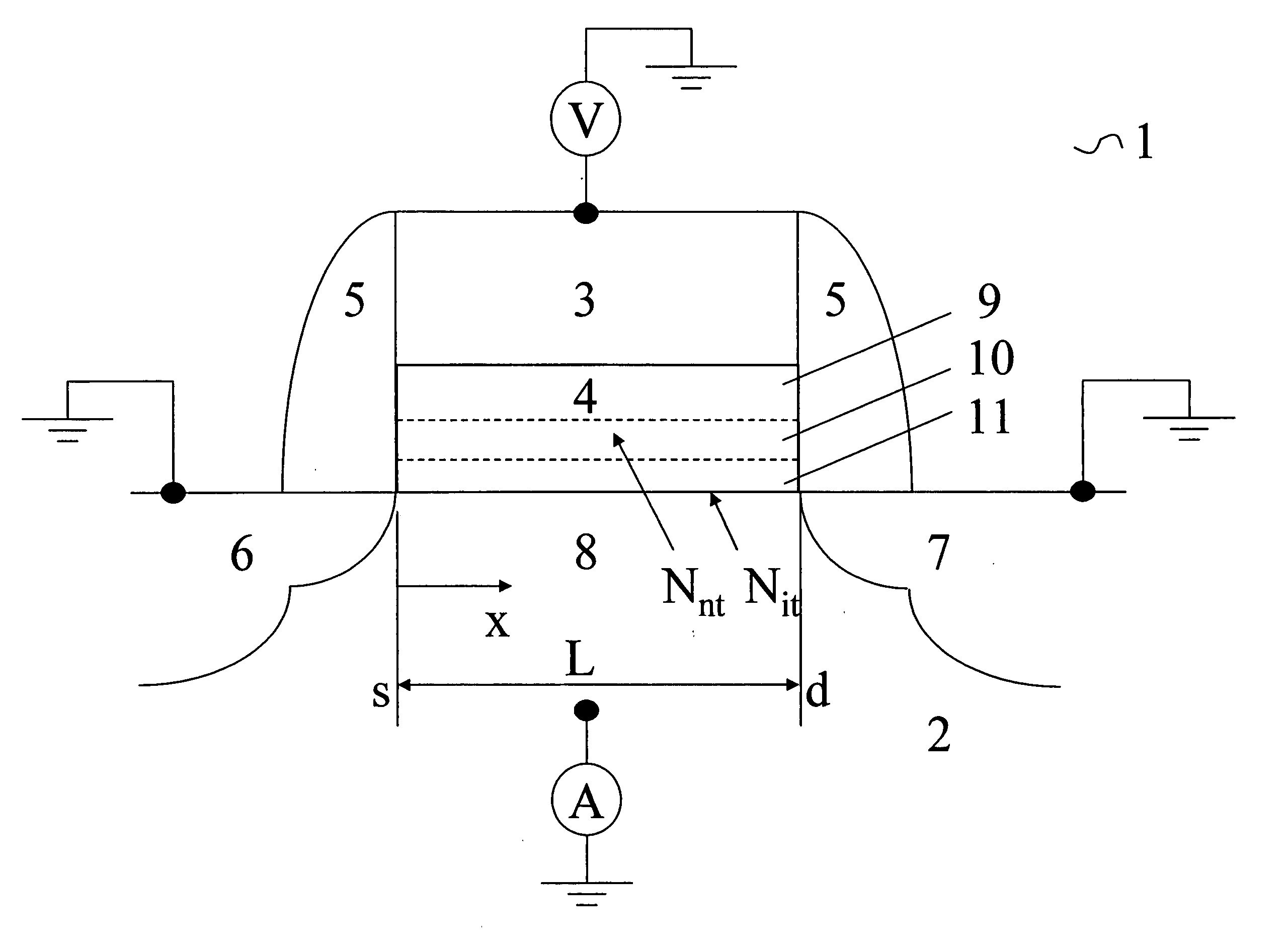
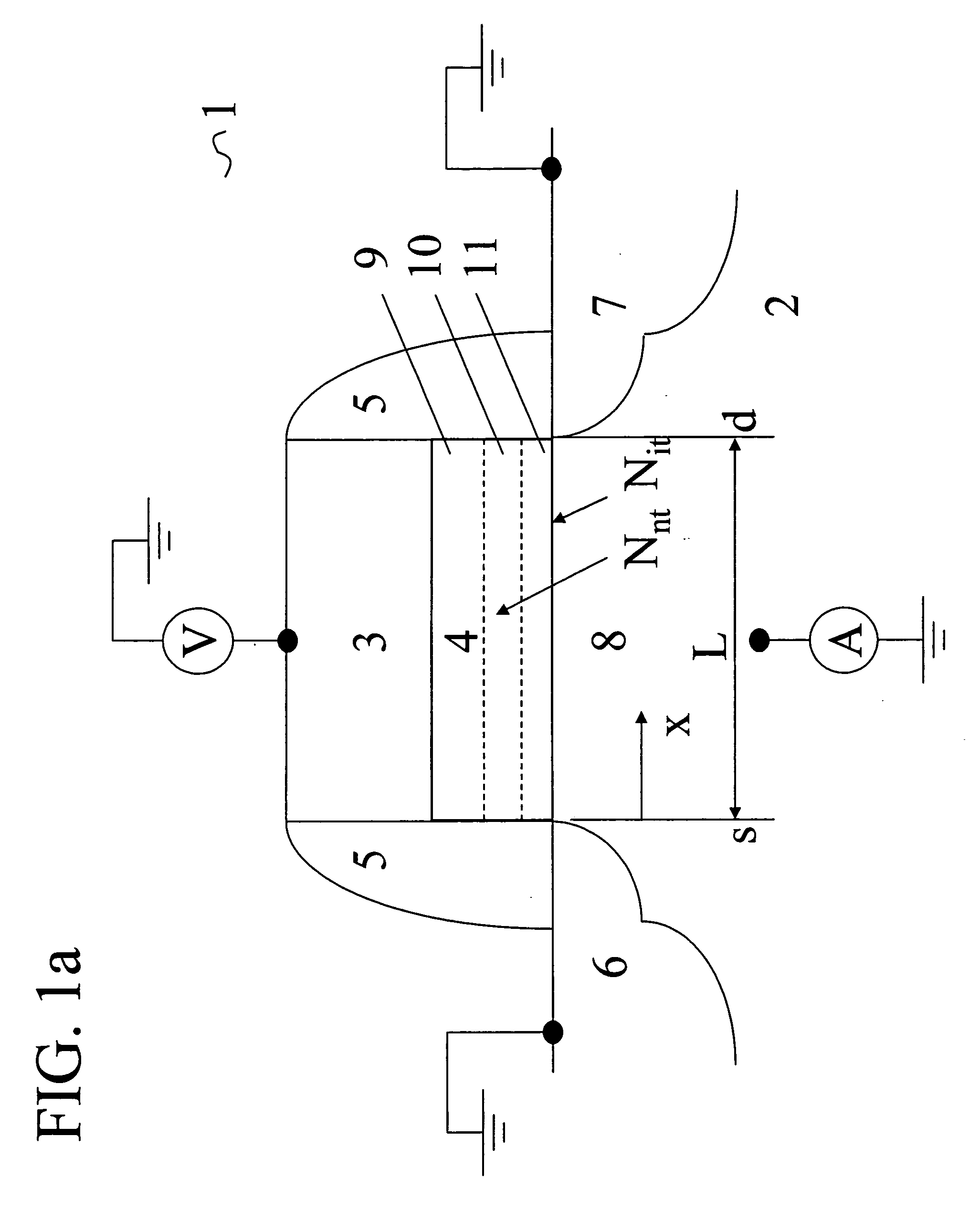
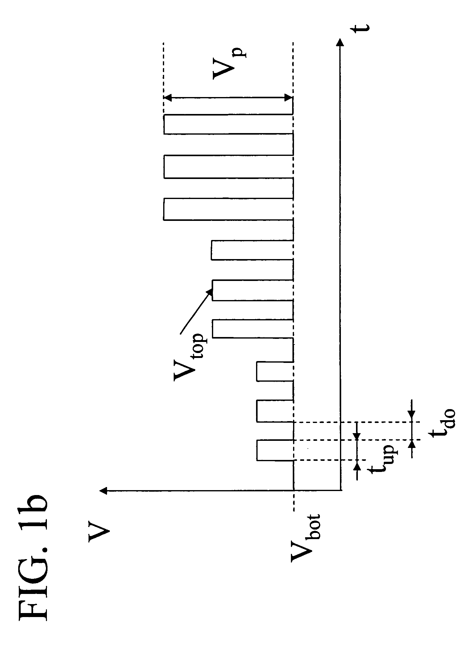
[0035] As described with reference to FIG. 1-8, a set of programming and erase conditions for operating a semiconductor device, preferably a non-volatile memory device comprising a charge-trapping layer, is determined.

[0036]FIG. 1 shows a schematic cross-section of such a semiconductor device, namely a MOSFET-type device. This device (1) comprises a gate electrode (3) separated from the substrate (2) by a gate dielectric (4). Typically the gate electrode is formed from a semiconductor material such as polycrystalline silicon doped to obtain the desired workfunction and / or conductivity. This semiconductor material can be partially or fully silicided as known in the art or even metals, e.g. Al, TiN, TaN, are used. The gate dielectric (8) comprises a dielectric charge-trapping layer (10) such as silicon-nitride, silicon-rich oxide, silicon-oxynitride, an oxide layer comprising nanocrystals of a semiconductor material, e.g. polycrystalline silicon. Optionally this charge-trapping layer...


PUM


Abstract

A method for determining programming / erase conditions and a method for operating a charge-trapping semiconductor device are disclosed. Programming and erase conditions are determined such that a first net charge distribution variation profile, upon going from programmed to erased state, is substantially the opposite of a second net charge distribution variation profile, upon going from erased to programmed state.

Description

[0001] The present application claims the priority of European Patent Application No. EP 05109602.2 (filed Oct. 14, 2005) and Provisional United States Application Nos. 60 / 704,859 (filed Aug. 1, 2005) and 60 / 687,076 (filed Jun. 3, 2005).BACKGROUND [0002] 1. Technical Field [0003] The present invention is in the field of semiconductor processing and devices, more specifically in the field of non-volatile charge-trapping memory devices. In particular, the present invention relates to a method for determining programming / erase conditions and a method for operating a non-volatile charge-trapping memory device. [0004] 2. Background Art [0005] Non-volatile memories (NVM) are characterized by the fact that once a bit is stored in a memory cell this bit will be retained even when the memory cell is no longer powered. When electrical fields are used for erasing and programming of the memory cell, the NVM devices are also known as EEPROM (Electrically-Erasable-and-Programmable-Read-Only-Memor...

Claims


Application Information

Patent Timeline
IPC IPC(8): G11C11/34
CPCG11C16/04G11C16/0475G11C16/26G11C2029/5002G11C16/3495G11C29/50G11C16/349
Inventor FURNEMONT, ARNAUD ADRIEN
Owner INTERUNIVERSITAIR MICRO ELECTRONICS CENT (IMEC VZW)
Why Eureka
Eureka Blog
Learn More